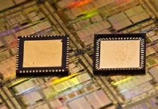
What is an IC Substrate?
An integrated circuit (IC) substrate is a thin board or base layer that provides mechanical support and electrical interconnections for semiconductor devices, such as microprocessors, memory chips, and other integrated circuits. The substrate acts as a foundation upon which the IC components are mounted, allowing them to be connected to each other and to external circuitry.
IC substrates are typically made from a dielectric material, such as ceramic, glass, or plastic, which provides insulation between the conductive layers. These conductive layers, usually made of copper, are patterned to form the necessary electrical connections between the IC components.
Importance of IC Substrates
IC substrates play a crucial role in the performance, reliability, and functionality of electronic devices. Some key reasons why IC substrates are essential include:
-
Mechanical support: IC substrates provide a stable base for the delicate semiconductor components, protecting them from physical damage and ensuring proper alignment.
-
Electrical interconnections: The conductive layers on the substrate allow electrical signals to be routed between the IC components and to external circuitry, enabling the device to function as intended.
-
Heat dissipation: IC substrates often incorporate features that help dissipate heat generated by the semiconductor components, preventing overheating and ensuring optimal performance.
-
Miniaturization: As electronic devices become smaller and more complex, IC substrates enable the dense packaging of components, allowing for more compact and efficient designs.

Types of IC Substrates
There are several types of IC substrates, each with its own characteristics and advantages. Some common types include:
1. Ceramic Substrates
Ceramic substrates are made from inorganic, non-metallic materials, such as alumina (Al2O3) or aluminum nitride (AlN). They offer excellent thermal conductivity, high mechanical strength, and good electrical insulation properties. Ceramic substrates are often used in high-power, high-frequency, and high-reliability applications, such as:
- Microwave and RF devices
- Power electronics
- Aerospace and defense systems
2. Organic Substrates
Organic substrates are made from polymer materials, such as bismaleimide triazine (BT) or FR-4. They are lighter, more flexible, and less expensive than ceramic substrates, making them popular for consumer electronics and other cost-sensitive applications. Some advantages of organic substrates include:
- Lower dielectric constant and loss tangent
- Ease of manufacturing and processing
- Compatibility with standard PCB assembly processes
3. Glass Substrates
Glass substrates, made from materials like borosilicate glass or fused silica, offer excellent dimensional stability, low dielectric loss, and high resistance to chemicals and moisture. They are often used in applications that require high precision and reliability, such as:
- MEMS (Micro-Electro-Mechanical Systems)
- Optical sensors and detectors
- Bio-compatible devices
4. Metal Core Substrates
Metal core substrates consist of a metal base layer, typically aluminum or copper, covered by a thin dielectric layer and conductive traces. The metal core provides excellent thermal conductivity, allowing for efficient heat dissipation. Metal core substrates are commonly used in high-power LED lighting and other applications that generate significant heat.

IC Substrate Manufacturing Process
The manufacturing process for IC substrates involves several key steps, which may vary depending on the substrate type and application. A typical process flow includes:
-
Raw material preparation: The substrate material, such as ceramic powder or polymer resin, is mixed and conditioned to achieve the desired properties.
-
Substrate formation: The raw material is shaped into a substrate using techniques like tape casting (for ceramics), lamination (for organic substrates), or cutting (for glass substrates).
-
Via formation: Holes are drilled or punched into the substrate to create vias, which will be used for vertical electrical connections between layers.
-
Metallization: Conductive layers, typically copper, are deposited onto the substrate using techniques like electroless plating, electroplating, or sputtering.
-
Patterning: The conductive layers are patterned using photolithography and etching processes to create the desired electrical interconnections.
-
Surface finishing: Additional surface treatments, such as solder mask application or surface plating (e.g., ENIG – Electroless Nickel Immersion Gold), are applied to protect the substrate and improve solderability.
-
Singulation: The substrate panel is cut into individual units, ready for component assembly and packaging.

IC Substrate Design Considerations
Designing an IC substrate involves several key considerations to ensure optimal performance, reliability, and manufacturability. Some important factors include:
1. Material Selection
The choice of substrate material depends on the application requirements, such as:
- Thermal conductivity
- Dielectric constant and loss tangent
- Mechanical strength and dimensional stability
- Cost and availability
2. Interconnect Design
The layout and routing of the conductive traces on the substrate must be carefully designed to:
- Minimize signal losses and distortion
- Control impedance and reduce crosstalk
- Ensure adequate current-carrying capacity
- Facilitate efficient component placement and assembly
3. Thermal Management
Proper thermal management is crucial for IC performance and reliability. Substrate design should consider:
- Incorporation of thermal vias or heat spreaders
- Selection of materials with appropriate thermal conductivity
- Optimization of component placement and power distribution
4. Manufacturing Constraints
The substrate design must be compatible with the chosen manufacturing process, taking into account factors such as:
- Minimum feature sizes (e.g., via diameter, trace width)
- Layer count and thickness limitations
- Material compatibility and adhesion
- Process tolerances and yield considerations
Advanced IC Substrate Technologies
As the demand for higher performance, smaller form factors, and greater functionality in electronic devices continues to grow, several advanced IC substrate technologies have emerged to address these challenges. Some notable examples include:
1. 2.5D and 3D Packaging
2.5D and 3D packaging technologies involve the vertical stacking of multiple IC chips or wafers, interconnected using through-silicon vias (TSVs) or interposers. These approaches enable higher density, shorter interconnects, and heterogeneous integration of different device technologies.
2. Embedded Components
Embedded component technology allows passive components, such as capacitors and resistors, to be integrated within the substrate itself, reducing the need for discrete components and saving space on the surface of the substrate.
3. High-Density Interconnect (HDI) Substrates
HDI substrates feature finer line widths, smaller vias, and higher layer counts compared to traditional substrates, enabling denser interconnections and more compact packaging.
4. Flexible and Stretchable Substrates
Flexible and stretchable substrates, made from materials like polyimide or elastomers, allow for the creation of bendable, conformable, and even wearable electronic devices.
Applications of IC Substrates
IC substrates find use in a wide range of electronic applications, from consumer devices to industrial and aerospace systems. Some common application areas include:
- Smartphones, tablets, and laptops
- Automotive electronics, such as infotainment systems and sensor modules
- Medical devices, like implantable sensors and wearable health monitors
- Industrial automation and control systems
- Telecommunications infrastructure, such as 5G base stations and data centers
- Aerospace and defense electronics, including satellites and avionics
Future Trends in IC Substrates
As the electronics industry continues to evolve, IC substrates will need to adapt to new challenges and opportunities. Some key trends shaping the future of IC substrates include:
-
Continued miniaturization: The demand for smaller, more compact electronic devices will drive the development of even finer-pitch interconnects and denser packaging technologies.
-
Integration of novel materials: New substrate materials, such as carbon nanotubes or graphene, may offer unique properties and performance advantages for specific applications.
-
Increased focus on sustainability: There will be a growing emphasis on environmentally friendly substrate materials and manufacturing processes, as well as the development of recyclable and biodegradable substrates.
-
Convergence with other technologies: IC substrates will play a crucial role in the integration of electronics with other technologies, such as photonics, MEMS, and bio-sensors, enabling new applications and functionalities.
FAQ
1. What is the difference between a PCB and an IC substrate?
While both PCBs and IC substrates provide mechanical support and electrical interconnections for electronic components, IC substrates are specifically designed to support and interconnect semiconductor devices, such as integrated circuits. PCBs, on the other hand, are used to connect and support a wider range of electronic components, including ICs, passive components, and connectors.
2. How do I select the right IC substrate material for my application?
Selecting the right IC substrate material depends on several factors, including:
- Thermal and electrical performance requirements
- Mechanical and environmental constraints
- Cost and manufacturability considerations
It is essential to consult with substrate suppliers and industry experts to determine the most suitable material for your specific application.
3. What is the role of vias in IC substrates?
Vias are vertical interconnections that allow electrical signals to pass through the layers of an IC substrate. They are essential for connecting the different conductive layers and enabling communication between the IC components mounted on the substrate.
4. How can I ensure the reliability of my IC substrate design?
To ensure the reliability of your IC substrate design, consider the following:
- Conduct thorough simulations and analyses to verify electrical and thermal performance
- Follow established design rules and guidelines for your chosen manufacturing process
- Perform accelerated life testing and environmental stress testing to validate long-term reliability
- Implement robust quality control and inspection processes during manufacturing
5. What are the challenges in adopting advanced IC substrate technologies?
Some challenges in adopting advanced IC substrate technologies include:
- Higher costs associated with new materials, processes, and equipment
- Increased complexity in design and manufacturing
- Limited availability of skilled personnel and knowledge resources
- Potential compatibility issues with existing supply chains and assembly processes
To overcome these challenges, it is crucial to collaborate with industry partners, invest in research and development, and foster a culture of continuous learning and innovation.
Conclusion
IC substrates are a critical component in modern electronics, providing the foundation for the integration and interconnection of semiconductor devices. As the demand for higher performance, smaller form factors, and greater functionality continues to grow, IC substrates will need to evolve to meet these challenges.
By understanding the types, manufacturing processes, design considerations, and advanced technologies associated with IC substrates, engineers and manufacturers can make informed decisions and drive innovation in this essential field. As the electronics industry advances, the role of IC substrates in enabling new applications and shaping the future of technology will only become more significant.
IC Substrate Comparison Table
| Substrate Type | Advantages | Disadvantages | Common Applications |
|---|---|---|---|
| Ceramic | – High thermal conductivity – High mechanical strength – Good electrical insulation |
– Brittle and fragile – Higher cost compared to organic substrates |
– Microwave and RF devices – Power electronics – Aerospace and defense systems |
| Organic | – Lower dielectric constant and loss tangent – Ease of manufacturing and processing – Compatibility with standard PCB assembly processes |
– Lower thermal conductivity compared to ceramic – Less dimensionally stable under heat and moisture |
– Consumer electronics – Automotive electronics – Telecommunications |
| Glass | – Excellent dimensional stability – Low dielectric loss – High resistance to chemicals and moisture |
– Brittle and fragile – Limited thermal conductivity |
– MEMS – Optical sensors and detectors – Bio-compatible devices |
| Metal Core | – Excellent thermal conductivity – Efficient heat dissipation |
– Higher cost compared to organic substrates – Limited electrical insulation properties |
– High-power LED lighting – Automotive power electronics |


Leave a Reply