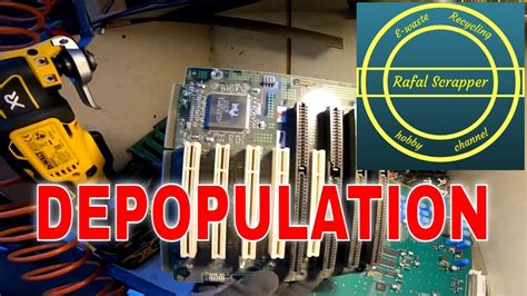
What is PCB Depopulation?
PCB depopulation refers to the process of removing electronic components and metals from printed circuit boards (PCBs). This is often done to recycle valuable metals like gold, silver, copper, and palladium from old or damaged PCBs. PCB depopulation can be performed manually or using automated equipment, depending on the scale and requirements of the operation.
Why Depopulate PCBs?
There are several reasons why PCBs are depopulated:
- Recycling valuable metals: PCBs contain precious metals like gold, silver, and palladium, which can be extracted and recycled for use in new electronic devices.
- Reducing electronic waste: By recovering metals from old PCBs, we can reduce the amount of electronic waste that ends up in landfills.
- Complying with regulations: Many countries have strict regulations regarding the disposal of electronic waste. PCB depopulation helps companies comply with these regulations.
Methods of PCB Depopulation
There are several methods used for PCB depopulation, each with its own advantages and disadvantages. The choice of method depends on factors such as the type of PCB, the components to be removed, and the scale of the operation.
Manual Depopulation
Manual depopulation involves removing components from PCBs by hand using tools like pliers, cutters, and Soldering Irons. This method is suitable for small-scale operations or for removing specific components from a PCB.
Advantages of Manual Depopulation
- Low initial investment
- Flexibility in selecting components to remove
- Suitable for small batches or specific components
Disadvantages of Manual Depopulation
- Time-consuming and labor-intensive
- Risk of damaging components or PCBs
- Not suitable for large-scale operations
Automated Depopulation
Automated depopulation involves using machines to remove components from PCBs. This method is faster and more efficient than manual depopulation, making it suitable for large-scale operations.
Types of Automated Depopulation Equipment
- Hot Air Rework Stations: These machines use hot air to melt the solder and remove components from PCBs.
- Infrared Rework Stations: These machines use infrared radiation to heat and remove components from PCBs.
- Solvent-Based Equipment: These machines use solvents to dissolve the solder and remove components from PCBs.
- Mechanical Equipment: These machines use mechanical force to remove components from PCBs, such as shearing or punching.
Advantages of Automated Depopulation
- Fast and efficient
- Suitable for large-scale operations
- Consistent results
- Reduced labor costs
Disadvantages of Automated Depopulation
- High initial investment
- Limited flexibility in selecting components to remove
- Potential damage to PCBs or components if not properly calibrated

The PCB Depopulation Process
The PCB depopulation process typically involves the following steps:
- Preparation: PCBs are sorted and prepared for depopulation. This may involve removing any plastics or other non-metallic components.
- Component Removal: Components are removed from the PCBs using manual or automated methods.
- Separation: The removed components are separated into different categories based on their material composition (e.g., ferrous metals, non-ferrous metals, plastics).
- Metallurgical Processing: The separated metals are then processed using metallurgical techniques to extract and purify the valuable metals.
PCB Depopulation Process Flow Chart
| Step | Description |
|---|---|
| 1 | PCB Preparation |
| 2 | Component Removal |
| 3 | Material Separation |
| 4 | Metallurgical Processing |

Safety Considerations in PCB Depopulation
PCB depopulation involves working with electronic waste, which can contain hazardous materials. It is essential to follow proper safety guidelines to protect workers and the environment.
Personal Protective Equipment (PPE)
Workers involved in PCB depopulation should wear appropriate PPE:
- Safety glasses or goggles
- Gloves (heat-resistant gloves for manual depopulation)
- Respirators or face masks
- Protective clothing
Environmental Considerations
PCB depopulation can generate hazardous waste, such as lead and other heavy metals. It is crucial to follow proper disposal methods and comply with environmental regulations.
- Use proper ventilation to control fumes and dust
- Collect and dispose of hazardous waste according to regulations
- Avoid releasing hazardous materials into the environment

Metals Recovered from PCBs
PCBs contain a variety of valuable metals that can be recovered through depopulation and metallurgical processing.
| Metal | Typical Content in PCBs (by weight) |
|---|---|
| Copper | 10-20% |
| Gold | 0.1-0.3% |
| Silver | 0.1-0.3% |
| Palladium | 0.01-0.05% |
| Tin | 1-5% |
| Lead | 1-5% |
Copper Recovery
Copper is the most abundant metal in PCBs, making up 10-20% of the total weight. Copper can be recovered through various methods, such as:
- Mechanical separation (e.g., shredding and sorting)
- Hydrometallurgical processes (e.g., leaching and electrowinning)
- Pyrometallurgical processes (e.g., smelting)
Precious Metal Recovery
PCBs contain small amounts of precious metals like gold, silver, and palladium. These metals can be recovered through processes such as:
- Chemical leaching
- Electrochemical recovery
- Pyrometallurgical processes
Economic Considerations in PCB Depopulation
The economic viability of PCB depopulation depends on several factors, including:
- The cost of the depopulation process
- The value of the recovered metals
- The scale of the operation
- Regulatory compliance costs
Factors Affecting Profitability
| Factor | Impact on Profitability |
|---|---|
| Metal prices | Higher metal prices increase profitability |
| Processing costs | Lower processing costs increase profitability |
| Regulatory compliance | Higher compliance costs reduce profitability |
| Scale of operation | Larger scale operations can be more profitable |
Frequently Asked Questions (FAQ)
-
Q: What is the difference between manual and automated PCB depopulation?
A: Manual depopulation involves removing components by hand using tools, while automated depopulation uses machines to remove components. Automated depopulation is faster and more efficient but requires a higher initial investment. -
Q: What safety precautions should be taken during PCB depopulation?
A: Workers should wear appropriate personal protective equipment (PPE) such as safety glasses, gloves, respirators, and protective clothing. Proper ventilation should be used to control fumes and dust, and hazardous waste should be disposed of according to regulations. -
Q: What are the most valuable metals found in PCBs?
A: The most valuable metals found in PCBs are typically gold, silver, and palladium. These precious metals are present in small amounts but have high economic value. -
Q: How can the profitability of PCB depopulation be improved?
A: Profitability can be improved by optimizing the depopulation process to reduce costs, increasing the scale of the operation, and ensuring compliance with regulations to avoid fines or penalties. Higher metal prices also contribute to increased profitability. -
Q: What happens to the metals recovered from PCBs?
A: The recovered metals are refined and purified using metallurgical processes. They can then be sold as raw materials for use in the production of new electronic devices or other applications that require these metals.
Conclusion
PCB depopulation is an important process for recovering valuable metals from old or damaged printed circuit boards, reducing electronic waste, and complying with environmental regulations. Both manual and automated methods can be used, depending on the scale and requirements of the operation. Safety considerations are crucial, as PCB depopulation involves working with potentially hazardous materials. The economic viability of PCB depopulation depends on factors such as metal prices, processing costs, regulatory compliance, and the scale of the operation. By optimizing the depopulation process and recovering valuable metals, we can contribute to a more sustainable and circular economy in the electronics industry.


Leave a Reply