What is PCB Panelization?
PCB panelization is the process of combining multiple small printed circuit boards (PCBs) onto a single larger panel for more efficient manufacturing. This technique is widely used in the electronics industry to reduce production costs, improve throughput, and streamline the assembly process. By grouping several PCBs together, manufacturers can optimize material usage, minimize handling, and speed up the fabrication and assembly stages.
Benefits of PCB Panelization
- Cost reduction
- Improved production efficiency
- Consistent quality
- Simplified handling and assembly
- Optimized material usage
Techniques for PCB Panelization
There are several methods for panelizing small PCBs, each with its own advantages and considerations. The choice of panelization technique depends on factors such as the PCB design, manufacturing requirements, and assembly process. Here are some common PCB panelization techniques:
1. Tab Routing
Tab routing involves connecting individual PCBs with thin tabs or strips of the PCB material. These tabs hold the boards together during manufacturing and are later removed during the depaneling process. Tab routing is a simple and cost-effective method for panelizing PCBs, making it a popular choice for low-volume production.
Advantages of Tab Routing
- Easy to implement
- Cost-effective for small production runs
- Minimal material waste
Disadvantages of Tab Routing
- Manual depaneling process
- Potential for damage during depaneling
- Limited to simple PCB designs
2. V-Scoring
V-scoring is a panelization technique that uses v-shaped grooves cut into the PCB panel to define the boundaries of individual boards. These grooves create weak points that allow for easy separation of the PCBs after manufacturing. V-scoring is an efficient method for panelizing boards with complex shapes or tight tolerances.
Advantages of V-Scoring
- Precise and clean separation of boards
- Suitable for complex PCB shapes
- Automated depaneling process
Disadvantages of V-Scoring
- Higher tooling costs compared to tab routing
- Potential for stress on components near the v-grooves
- Limited board thickness options
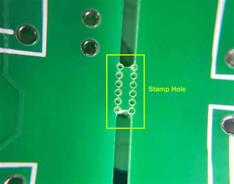
3. Perforated Boards
Perforated board panelization involves creating a series of small, closely spaced holes along the edges of individual PCBs. These perforations weaken the panel, allowing for easy separation of the boards after manufacturing. This technique is well-suited for high-volume production and can be combined with other panelization methods for optimal results.
Advantages of Perforated Boards
- Suitable for high-volume production
- Compatible with automated assembly processes
- Can be combined with other panelization methods
Disadvantages of Perforated Boards
- Increased design complexity
- Higher tooling costs
- Potential for damage during depaneling

Designing for PCB Panelization
To ensure successful panelization of small PCBs, it is essential to consider panelization requirements during the design phase. Here are some key factors to keep in mind when designing PCBs for panelization:
1. Board Spacing
Adequate spacing between individual PCBs on the panel is crucial for proper panelization. This spacing, known as the “route” or “web,” should be wide enough to accommodate the chosen panelization technique and ensure the structural integrity of the panel during manufacturing.
2. Component Placement
When placing components on the PCB, consider their proximity to the edges of the board and the panelization method being used. Components should be placed at a safe distance from the edges to prevent damage during the panelization and depaneling processes.
3. Fiducial Marks
Fiducial marks are reference points used by automated assembly equipment to accurately position and orient the PCBs during the manufacturing process. Including fiducial marks in your PCB design is essential for ensuring proper alignment and consistent results when panelizing boards.
4. Tooling Holes
Tooling holes are used to secure the PCB panel during the manufacturing process. These holes should be positioned accurately and sized according to the requirements of the manufacturing equipment. Proper placement of tooling holes helps to maintain the stability and alignment of the panel throughout the fabrication process.
5. Panelization Method Compatibility
When designing PCBs for panelization, it is important to choose a panelization method that is compatible with your board design and manufacturing requirements. Consider factors such as board shape, size, thickness, and component placement when selecting a panelization technique to ensure optimal results.

Panelization Design Tools
To streamline the panelization design process, there are various software tools available that allow you to create and optimize PCB panel layouts. These tools often include features such as automatic panel creation, design rule checking, and compatibility with popular PCB design software. Some popular panelization design tools include:
- PCB Panelizer
- PanelCreator
- DFMPro
- InPack
These tools can help you save time and reduce errors when designing PCB panels, ensuring that your designs are optimized for manufacturability and cost-effectiveness.

PCB Panelization Best Practices
To achieve the best results when panelizing small PCBs, consider the following best practices:
- Minimize material waste by optimizing panel layout and utilizing the available space effectively.
- Ensure consistent board spacing and alignment to facilitate automated assembly processes.
- Use appropriate panelization techniques based on your PCB design, manufacturing requirements, and production volume.
- Incorporate fiducial marks and tooling holes in your PCB design to ensure accurate positioning and alignment during manufacturing.
- Test your panelization design before mass production to identify and address any potential issues.
By following these best practices and carefully considering your panelization requirements during the design phase, you can ensure successful and cost-effective manufacturing of your small PCBs.
Frequently Asked Questions (FAQ)
1. What is the minimum spacing required between PCBs on a panel?
The minimum spacing between PCBs on a panel depends on the panelization method being used and the manufacturing capabilities of your chosen fabricator. Generally, a spacing of 2-3 mm is recommended for tab routing, while v-scoring and perforated board panelization may require slightly larger spacing. Consult with your fabricator to determine the optimal spacing for your specific project.
2. Can I mix different PCB designs on the same panel?
Yes, it is possible to include different PCB designs on the same panel, as long as they share similar manufacturing specifications (e.g., board thickness, copper weight, and surface finish). This approach, known as “mixed-panel panelization,” can help to reduce production costs and minimize material waste. However, it is essential to ensure that the different designs do not interfere with each other during the panelization and depaneling processes.
3. How do I choose the best panelization method for my project?
Choosing the best panelization method for your project depends on several factors, including your PCB design, manufacturing requirements, production volume, and budget. Tab routing is often the most cost-effective option for low-volume production and simple PCB designs, while v-scoring and perforated board panelization are better suited for more complex designs and higher production volumes. Consider consulting with your fabricator or an experienced PCB designer to determine the most appropriate panelization method for your specific project.
4. Can I panelize PCBs with different thicknesses on the same panel?
While it is technically possible to panelize PCBs with different thicknesses on the same panel, it is generally not recommended. Varying board thicknesses can lead to uneven pressure distribution during the lamination process, resulting in poor bonding and potential delamination issues. Additionally, different board thicknesses may require different depths for v-scoring or perforations, complicating the panelization process. It is best to panelize PCBs with the same thickness to ensure consistent manufacturing quality and reliability.
5. How do I ensure that my PCB design is compatible with panelization?
To ensure that your PCB design is compatible with panelization, consider the following factors:
- Include adequate spacing between individual PCBs on the panel to accommodate the chosen panelization method.
- Place components at a safe distance from the edges of the board to prevent damage during panelization and depaneling.
- Incorporate fiducial marks and tooling holes in your design to ensure accurate positioning and alignment during manufacturing.
- Choose a panelization method that is compatible with your board shape, size, thickness, and component placement.
- Consult with your fabricator or an experienced PCB designer to review your design and ensure its compatibility with panelization.
By addressing these factors during the design phase, you can minimize potential issues and ensure the successful panelization of your small PCBs.
| Panelization Technique | Advantages | Disadvantages |
|---|---|---|
| Tab Routing | – Easy to implement – Cost-effective for small production runs – Minimal material waste |
– Manual depaneling process – Potential for damage during depaneling – Limited to simple PCB designs |
| V-Scoring | – Precise and clean separation of boards – Suitable for complex PCB shapes – Automated depaneling process |
– Higher tooling costs compared to tab routing – Potential for stress on components near the v-grooves – Limited board thickness options |
| Perforated Boards | – Suitable for high-volume production – Compatible with automated assembly processes – Can be combined with other panelization methods |
– Increased design complexity – Higher tooling costs – Potential for damage during depaneling |
In conclusion, panelizing small PCBs is an essential process for optimizing manufacturing efficiency, reducing costs, and improving overall product quality. By understanding the various panelization techniques, designing with panelization in mind, and following best practices, you can ensure the successful fabrication and assembly of your small PCBs. Collaborating with experienced fabricators and PCB designers can help you navigate the panelization process and achieve the best results for your specific project requirements.


Leave a Reply