Introduction to PCB Panelization
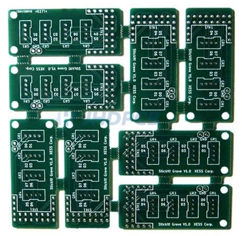
PCB panelization is the process of grouping multiple printed circuit board (PCB) designs onto a single panel for manufacturing. This technique is commonly used to increase production efficiency and reduce costs. When dealing with round-shaped PCBs, panelization can be particularly challenging due to their unique geometry. In this article, we will explore the various methods and considerations for panelizing round-shaped PCBs effectively.
Understanding the Challenges of Round-Shaped PCB Panelization
Round-shaped PCBs present several challenges when it comes to panelization:
- Inefficient space utilization: Unlike rectangular PCBs, round-shaped PCBs do not tessellate perfectly, leading to wasted panel space.
- Difficulty in panel routing: The curved edges of round-shaped PCBs require specialized routing techniques to ensure proper separation and minimize material waste.
- Increased fabrication complexity: Panelizing round-shaped PCBs often involves more intricate fabrication processes, such as v-scoring or tab routing, which can increase production time and costs.
Despite these challenges, panelizing round-shaped PCBs is essential for many applications, such as wearable devices, IoT sensors, and medical equipment.

Panelization Techniques for Round-Shaped PCBs
Several techniques can be employed to panelize round-shaped PCBs effectively:
V-Scoring
V-scoring is a popular method for panelizing round-shaped PCBs. It involves creating v-shaped grooves along the perimeter of each individual PCB, allowing for easy separation after fabrication. The depth and angle of the v-score must be carefully calculated to ensure clean breakaway without damaging the PCBs.
Advantages of v-scoring:
– Enables precise and clean separation of individual PCBs
– Minimizes material waste compared to tab routing
– Suitable for high-volume production
Disadvantages of v-scoring:
– Requires specialized equipment and tooling
– May increase fabrication costs
– Limited to certain PCB Thicknesses and materials
Tab Routing
Tab routing is another common technique for panelizing round-shaped PCBs. It involves leaving small tabs or bridges connecting the individual PCBs to the panel frame. These tabs are later broken off to separate the PCBs after fabrication.
Advantages of tab routing:
– Simpler and more cost-effective compared to v-scoring
– Suitable for low to medium-volume production
– Allows for more flexibility in panel design
Disadvantages of tab routing:
– Manual separation of PCBs can be time-consuming
– Risk of damaging PCBs during the separation process
– May leave visible tab residue on the final product
Combination of V-Scoring and Tab Routing
In some cases, a combination of v-scoring and tab routing can be used to panelize round-shaped PCBs. This approach involves creating v-scores along the curved edges of the PCBs and using tabs to connect them to the panel frame. This hybrid method offers the benefits of both techniques while mitigating their individual drawbacks.

Design Considerations for Panelizing Round-Shaped PCBs
When panelizing round-shaped PCBs, several design considerations must be taken into account:
Panel Layout and Orientation
Optimizing the panel layout is crucial for maximizing space utilization and minimizing material waste. Consider the following factors:
- Arrangement of PCBs on the panel
- Orientation of PCBs to minimize wasted space
- Spacing between individual PCBs to allow for proper separation
- Inclusion of fiducial marks for alignment and registration
Panelization Borders and Clearances
Adequate borders and clearances must be maintained around each PCB to ensure proper separation and prevent damage during the panelization process. Consider the following guidelines:
- Minimum border width around each PCB
- Clearance between PCBs and panel edges
- Clearance between PCBs and any panelization features (e.g., v-scores, tabs)
Panelization Feature Design
The design of panelization features, such as v-scores or tabs, is critical for successful separation of individual PCBs. Consider the following factors:
- Depth and angle of v-scores
- Width and length of tabs
- Placement of panelization features to minimize stress on PCBs during separation
- Material properties and thickness of the PCB substrate
Tooling and Fabrication Constraints
When panelizing round-shaped PCBs, it is essential to consider the capabilities and constraints of the fabrication process and tooling. Consult with your PCB manufacturer to determine:
- Maximum panel size and thickness
- Minimum feature sizes and tolerances
- Available panelization techniques and equipment
- Any specific design rules or guidelines for panelization

Best Practices for Panelizing Round-Shaped PCBs
To ensure successful panelization of round-shaped PCBs, follow these best practices:
-
Collaborate with your PCB manufacturer: Engage your PCB manufacturer early in the design process to discuss panelization requirements, constraints, and recommendations.
-
Optimize panel layout: Experiment with different panel layouts and orientations to maximize space utilization and minimize material waste.
-
Use appropriate panelization techniques: Select the most suitable panelization technique (e.g., v-scoring, tab routing, or a combination) based on your specific requirements, production volume, and budget.
-
Maintain proper clearances and borders: Ensure adequate clearances and borders around each PCB to prevent damage during the panelization process and facilitate clean separation.
-
Incorporate fiducial marks: Include fiducial marks on the panel to aid in alignment and registration during fabrication and assembly.
-
Test and validate the panelization design: Perform thorough testing and validation of the panelization design to identify and address any issues before mass production.
Frequently Asked Questions (FAQ)
-
Q: What is the minimum border width required around each PCB in a panel?
A: The minimum border width depends on the specific panelization technique and PCB manufacturer’s guidelines. Typically, a border width of 3-5 mm is recommended for v-scoring, while tab routing may require a larger border of 5-10 mm. -
Q: Can I panelize round-shaped PCBs of different sizes on the same panel?
A: Yes, it is possible to panelize round-shaped PCBs of different sizes on the same panel. However, it may require careful planning and optimization of the panel layout to ensure proper spacing and separation of individual PCBs. -
Q: How do I determine the appropriate depth and angle for v-scoring?
A: The depth and angle of v-scores depend on the PCB thickness and material properties. Generally, a v-score depth of 1/3 to 1/2 of the PCB thickness is recommended, with an angle between 30° and 60°. Consult with your PCB manufacturer for specific guidelines. -
Q: Is it possible to panelize round-shaped PCBs with different thicknesses on the same panel?
A: Panelizing round-shaped PCBs with different thicknesses on the same panel is not recommended, as it can lead to uneven stress distribution during the separation process and increase the risk of PCB Damage. It is best to panelize PCBs of the same thickness on a single panel. -
Q: How can I minimize the risk of damaging PCBs during the separation process?
A: To minimize the risk of damaging PCBs during separation, ensure proper design of panelization features (e.g., v-scores or tabs), maintain adequate clearances and borders, and use appropriate tools and techniques for separating the PCBs. Engaging with your PCB manufacturer for guidance and support can also help reduce the risk of damage.
Conclusion
Panelizing round-shaped PCBs presents unique challenges due to their non-rectangular geometry. However, with careful planning, appropriate techniques, and consideration of design factors, it is possible to panelize round-shaped PCBs effectively. V-scoring and tab routing are common methods for panelizing round-shaped PCBs, each with its advantages and disadvantages. Optimizing panel layout, maintaining proper clearances and borders, and collaborating with your PCB manufacturer are essential for successful panelization.
By following best practices and considering the specific requirements of your project, you can efficiently panelize round-shaped PCBs, reduce production costs, and ensure the quality of your final product.
| Panelization Technique | Advantages | Disadvantages |
|---|---|---|
| V-Scoring | – Precise and clean separation – Minimizes material waste – Suitable for high-volume production |
– Requires specialized equipment and tooling – May increase fabrication costs – Limited to certain PCB thicknesses and materials |
| Tab Routing | – Simpler and more cost-effective – Suitable for low to medium-volume production – Allows for more flexibility in panel design |
– Manual separation can be time-consuming – Risk of damaging PCBs during separation – May leave visible tab residue on the final product |
By understanding the challenges, techniques, and design considerations involved in panelizing round-shaped PCBs, you can make informed decisions and optimize your manufacturing process for success.


Leave a Reply