Introduction to PCB Printing
Printed Circuit Board (PCB) printing is a crucial step in the manufacturing process of electronic devices. It involves creating a pattern of conductive tracks, pads, and other features onto a substrate material, typically fiberglass or plastic. Proper PCB printing ensures that the electronic components are correctly connected and the device functions as intended.
In this article, we will discuss the various aspects of PCB printing and provide a comprehensive guide on how to ensure that the printing process is carried out properly.
Understanding the PCB Printing Process
Types of PCB Printing
There are several methods used for PCB printing, each with its own advantages and limitations. The most common types of PCB printing are:
-
Screen Printing: This method uses a stencil to apply ink or paste onto the PCB surface. It is suitable for low-volume production and prototyping.
-
Inkjet Printing: This method uses a special inkjet printer to deposit conductive ink onto the PCB surface. It offers high precision and is suitable for small-scale production.
-
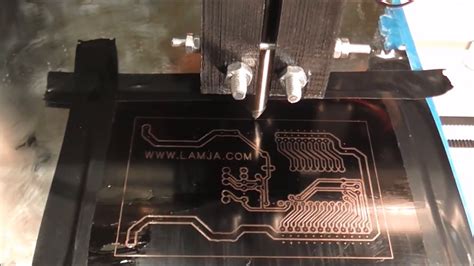
Photoengraving: This method involves using a photoresist material and UV light to create a pattern on the PCB surface. It is suitable for high-volume production and offers excellent resolution.
PCB Printing Materials
The choice of materials used in PCB printing depends on the specific requirements of the project. Some common materials used in PCB printing include:
| Material | Description | Advantages | Limitations |
|---|---|---|---|
| Copper | A conductive metal used for creating tracks and pads | Excellent conductivity, durability | Expensive, prone to oxidation |
| Solder Mask | A layer of polymer applied over the copper to protect it from oxidation and short circuits | Improves reliability, protects against environmental factors | Adds complexity to the manufacturing process |
| Silkscreen | A layer of ink used for labeling components and providing visual guides | Enhances usability, improves aesthetics | Limited resolution, can wear off over time |
PCB Printing Equipment
The equipment used in PCB printing varies depending on the specific method and scale of production. Some common equipment used in PCB printing includes:
- Screen printing machines
- Inkjet printers
- Photoengraving equipment
- Etching tanks
- Drills and routers

Ensuring Proper PCB Printing
Design Considerations
Proper PCB printing starts with a well-designed PCB layout. Some key design considerations include:
-
Track Width and Spacing: The width and spacing of the conductive tracks should be appropriate for the current carrying capacity and signal integrity requirements of the circuit.
-
Pad Size and Shape: The size and shape of the pads should be appropriate for the components being used and the soldering method employed.
-
Drill Holes: The size and placement of drill holes should be accurate to ensure proper component placement and connectivity.
-
Solder Mask and Silkscreen: The solder mask and silkscreen layers should be designed to provide adequate protection and labeling for the components and tracks.
Pre-Printing Preparation
Before the actual printing process begins, several preparatory steps need to be taken to ensure proper PCB printing:
-
Cleaning: The PCB substrate should be thoroughly cleaned to remove any dirt, grease, or contamination that could affect the printing process.
-
Inspection: The PCB substrate should be inspected for any defects or irregularities that could impact the printing quality.
-
Alignment: The PCB substrate should be properly aligned with the printing equipment to ensure accurate placement of the conductive tracks and pads.
Printing Process Control
During the actual printing process, several factors need to be monitored and controlled to ensure proper PCB printing:
-
Ink/Paste Viscosity: The viscosity of the ink or paste used in the printing process should be maintained within the recommended range to ensure proper flow and adhesion.
-
Print Pressure: The pressure applied during the printing process should be controlled to ensure even distribution of the ink or paste and avoid smudging or bleeding.
-
Print Speed: The speed of the printing process should be optimized to ensure adequate coverage and avoid defects such as skipping or overprinting.
-
Curing: After printing, the ink or paste should be properly cured to ensure good adhesion and conductivity.
Post-Printing Inspection
After the printing process is complete, the PCB should be inspected to ensure that the printing quality meets the required standards. Some common inspection methods include:
-
Visual Inspection: The PCB is visually inspected for any defects such as smudging, bleeding, or incomplete coverage.
-
Automated Optical Inspection (AOI): An automated system is used to scan the PCB and detect any defects or irregularities.
-
Electrical Testing: The PCB is tested for electrical continuity and functionality to ensure that the printed tracks and pads are properly connected.

Common PCB Printing Defects and How to Avoid Them
Despite the best efforts to control the printing process, defects can still occur. Some common PCB printing defects and how to avoid them include:
-
Overprinting: This occurs when too much ink or paste is applied, leading to smudging or bleeding. It can be avoided by controlling the print pressure and viscosity.
-
Underprinting: This occurs when too little ink or paste is applied, leading to incomplete coverage or broken tracks. It can be avoided by ensuring adequate ink/paste supply and controlling the print speed.
-
Misalignment: This occurs when the printed pattern is not properly aligned with the PCB substrate, leading to incorrect component placement or connectivity issues. It can be avoided by ensuring proper alignment of the PCB substrate and printing equipment.
-
Contamination: This occurs when foreign particles or contaminants are introduced into the printing process, leading to defects or poor adhesion. It can be avoided by maintaining a clean printing environment and properly cleaning the PCB substrate before printing.

Frequently Asked Questions (FAQ)
-
What is the best method for PCB printing?
The best method for PCB printing depends on the specific requirements of the project, such as the complexity of the design, the volume of production, and the available resources. Screen printing is suitable for low-volume production and prototyping, while photoengraving is better suited for high-volume production and high-resolution designs. -
How can I ensure proper alignment of the PCB substrate and printing equipment?
Proper alignment can be ensured by using alignment marks or fiducials on the PCB substrate and printing equipment. These marks are used to precisely position the PCB substrate relative to the printing equipment, ensuring accurate placement of the printed pattern. -
What is the recommended viscosity range for PCB printing ink or paste?
The recommended viscosity range for PCB printing ink or paste varies depending on the specific printing method and equipment being used. Generally, a viscosity range of 50-100 Pa·s is suitable for screen printing, while a range of 10-30 Pa·s is suitable for inkjet printing. -
How can I test the electrical functionality of a printed PCB?
Electrical functionality of a printed PCB can be tested using various methods such as continuity testing, resistance measurement, and functional testing. Continuity testing checks for proper connectivity between the printed tracks and pads, while resistance measurement verifies that the tracks have the correct electrical resistance. Functional testing involves powering up the PCB and verifying that it performs the intended functions. -
What are some common causes of contamination in the PCB printing process?
Common causes of contamination in the PCB printing process include dust, grease, oils, and other foreign particles that can be introduced from the environment, equipment, or handling. Contamination can also occur from residues left behind from previous processing steps, such as etching or plating. Proper cleaning and maintenance of the printing environment and equipment can help minimize the risk of contamination.
Conclusion
PCB printing is a critical step in the manufacturing process of electronic devices, and ensuring proper printing is essential for the functionality and reliability of the final product. By understanding the various aspects of PCB printing, including the different printing methods, materials, and equipment, as well as the key design considerations and process control factors, manufacturers can optimize their PCB printing process and minimize the risk of defects.
Proper pre-printing preparation, process control, and post-printing inspection are all essential for ensuring the quality of the printed PCB. By following best practices and staying up-to-date with the latest technologies and techniques, manufacturers can achieve high-quality PCB printing results and deliver reliable electronic products to their customers.


Leave a Reply