Introduction to PCB Assembly
PCB assembly is the process of populating a printed circuit board (PCB) with electronic components to create a functional electronic device. The PCB serves as the foundation for the electronic circuit, providing the necessary electrical connections between components. The assembly process involves several steps, including solder paste application, component placement, soldering, and inspection.
Key Components in PCB Assembly
- PCB (Printed Circuit Board)
- Electronic components (resistors, capacitors, integrated circuits, etc.)
- Solder paste
- Pick-and-place machine
- Reflow oven
- Inspection equipment (automated optical inspection, X-ray inspection)
PCB Assembly Process Flow
The PCB assembly process typically follows these steps:
- Solder Paste Application
- Component Placement
- Soldering
- Inspection and Testing
- Cleaning and Finishing
Step 1: Solder Paste Application
Solder paste is a mixture of tiny solder particles suspended in a flux medium. It is applied to the PCB’s surface using a stencil or screen printing process. The stencil is a thin metal sheet with openings that correspond to the PCB’s solder pads. The solder paste is spread over the stencil, filling the openings and depositing the paste onto the solder pads.
Solder Paste Composition
| Component | Description |
|---|---|
| Solder Particles | Tiny metal alloy balls, typically made of tin, lead, and silver |
| Flux | A chemical agent that helps remove oxides and promotes solder wetting |
| Solvents | Used to control the viscosity and rheology of the solder paste |
| Additives | Substances that improve the solder paste’s performance and shelf life |
Step 2: Component Placement
After the solder paste is applied, the electronic components are placed onto the PCB. This process is usually done using a pick-and-place machine, which automatically picks up components from feeders and places them onto the PCB with high precision.
Types of Component Packages
| Package Type | Description |
|---|---|
| Through-Hole | Components with leads that are inserted into holes drilled in the PCB |
| Surface Mount (SMD) | Components that are placed directly onto the PCB’s surface |
| Ball Grid Array (BGA) | ICs with an array of solder balls underneath for high-density connections |
| Quad Flat Package (QFP) | ICs with leads extending from all four sides of the package |
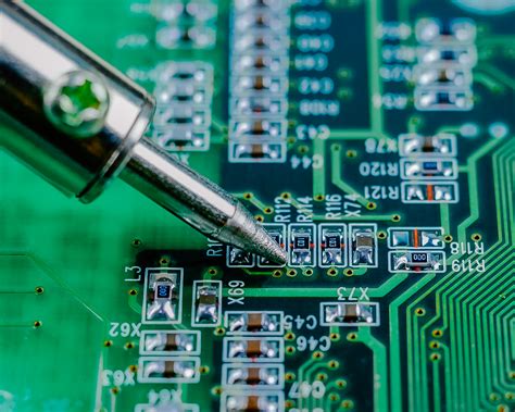
Step 3: Soldering
Once the components are placed, the PCB goes through a soldering process to create permanent electrical connections. The most common method for PCB assembly is reflow soldering, which involves heating the entire PCB in a reflow oven. The solder paste melts and forms a strong bond between the components and the PCB’s solder pads.
Reflow Soldering Profile
A typical reflow soldering profile consists of four stages:
- Preheat: The PCB is gradually heated to activate the flux and remove solvents.
- Soak: The temperature is maintained to ensure even heating and flux activation.
- Reflow: The temperature is increased above the solder’s melting point, allowing the solder to form connections.
- Cooling: The PCB is cooled down to allow the solder joints to solidify.
Step 4: Inspection and Testing
After soldering, the PCB undergoes inspection and testing to ensure the quality of the assembly. This step is crucial for identifying any defects or issues that may affect the PCB’s functionality.
Common Inspection Methods
- Visual Inspection: A manual or automated visual check for obvious defects, such as missing components or solder bridges.
- Automated Optical Inspection (AOI): An automated system that uses cameras and image processing algorithms to detect assembly defects.
- X-Ray Inspection: Used for inspecting solder joints underneath BGA Components or other hidden connections.
- In-Circuit Testing (ICT): A test that verifies the PCB’s functionality by applying electrical signals and measuring responses.
- Functional Testing: A test that verifies the PCB’s performance under real-world operating conditions.
Step 5: Cleaning and Finishing
After inspection and testing, the PCB may undergo cleaning to remove any residual flux or contaminants. This step is essential for ensuring the long-term reliability of the electronic device. Common cleaning methods include:
- Aqueous Cleaning: Using water-based solutions to remove flux residues.
- Solvent Cleaning: Using chemical solvents to dissolve and remove contaminants.
- No-Clean: Using low-residue flux that does not require cleaning.
Finally, the PCB may go through additional finishing steps, such as conformal coating, potting, or encapsulation, depending on the application requirements.

Benefits of Automated PCB Assembly
Automated PCB assembly offers several advantages over manual assembly:
- Higher Throughput: Automated systems can place components and solder PCBs much faster than manual methods.
- Improved Accuracy: Pick-and-place machines and automated soldering systems offer high precision and consistency.
- Reduced Labor Costs: Automation reduces the need for manual labor, leading to cost savings.
- Better Quality Control: Automated Inspection methods can detect defects more reliably than manual inspection.
- Increased Flexibility: Automated systems can be easily reconfigured for different PCB designs and components.

Challenges in PCB Assembly
Despite the advantages of automated PCB assembly, there are still some challenges that manufacturers face:
- Component Miniaturization: As electronic devices become smaller, the components and PCBs also shrink, making assembly more challenging.
- High-Mix, Low-Volume Production: Manufacturers often need to assemble a wide variety of PCBs in small quantities, requiring frequent changeovers and setup times.
- Counterfeit Components: The proliferation of counterfeit electronic components poses a risk to the quality and reliability of PCB assemblies.
- Environmental Regulations: Manufacturers must comply with regulations regarding the use of hazardous substances, such as lead and certain solvents.
- Supply Chain Management: Ensuring a stable supply of components and materials is crucial for maintaining production schedules and quality.

Future Trends in PCB Assembly
As technology advances, PCB assembly processes are evolving to keep pace with new requirements and challenges:
- 3D Printing: Additive manufacturing techniques are being explored for creating PCBs and even embedding components within the board.
- Flexible and Stretchable Electronics: The demand for wearable devices and IoT applications is driving the development of flexible and stretchable PCBs.
- Advanced Materials: New materials, such as graphene and carbon nanotubes, are being investigated for their potential in creating high-performance PCBs.
- Artificial Intelligence and Machine Learning: AI and ML algorithms are being applied to optimize PCB assembly processes, improve quality control, and predict maintenance needs.
- Sustainability and Circular Economy: Manufacturers are focusing on reducing waste, increasing recycling, and adopting more environmentally friendly materials and processes.
Conclusion
PCB assembly is a complex process that involves multiple steps and technologies. By understanding the various stages of PCB assembly, from solder paste application to inspection and finishing, manufacturers can optimize their processes for quality, efficiency, and cost-effectiveness. As electronic devices continue to evolve, PCB assembly will need to adapt to new challenges and opportunities, embracing advanced technologies and sustainable practices.
Frequently Asked Questions (FAQ)
1. What is the difference between through-hole and surface mount components?
Through-hole components have leads that are inserted into holes drilled in the PCB, while surface mount components are placed directly onto the PCB’s surface. Surface mount technology allows for smaller components and higher component density, but through-hole components are still used for certain applications, such as high-power devices or connectors.
2. What is the purpose of solder paste in PCB assembly?
Solder paste is a mixture of tiny solder particles and flux that is applied to the PCB’s solder pads before component placement. The solder particles provide the material for creating the electrical connections between the components and the PCB, while the flux helps remove oxides and promote solder wetting during the soldering process.
3. How does reflow soldering work?
Reflow soldering is a process where the entire PCB is heated in a reflow oven to melt the solder paste and create permanent electrical connections. The PCB goes through a temperature profile that includes preheat, soak, reflow, and cooling stages. The solder paste melts during the reflow stage, forming strong bonds between the components and the PCB’s solder pads.
4. What are some common methods for inspecting PCB assemblies?
Common inspection methods for PCB assemblies include visual inspection, automated optical inspection (AOI), X-ray inspection, in-circuit testing (ICT), and functional testing. Visual inspection is a manual or automated check for obvious defects, while AOI uses cameras and image processing algorithms to detect assembly defects. X-ray inspection is used for examining solder joints underneath components, and ICT and functional testing verify the PCB’s electrical functionality.
5. What are some challenges in PCB assembly, and how are they being addressed?
Some challenges in PCB assembly include component miniaturization, high-mix low-volume production, counterfeit components, environmental regulations, and supply chain management. Manufacturers are addressing these challenges by adopting advanced technologies, such as 3D printing, flexible and stretchable electronics, and advanced materials. They are also applying artificial intelligence and machine learning to optimize processes and improve quality control, while focusing on sustainability and circular economy practices.


Leave a Reply