What is PCB Stackup?
PCB stackup refers to the arrangement of copper and insulating layers that make up a printed circuit board (PCB). It defines the number of layers, their order, thickness, and materials. The stackup design is crucial for ensuring proper functionality, signal integrity, and manufacturability of the PCB.
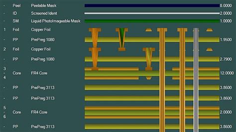
Key Components of a PCB Stackup
- Copper Layers:
- Signal layers: Used for routing traces that carry electrical signals
-
Power and ground planes: Provide stable voltage references and return paths for signals
-
Insulating Layers:
- Core: Thick, rigid insulating material that provides structural support
-
Prepreg: Thin, semi-cured insulating material used to bond layers together
-
Solder Mask: Protective coating applied to the outer layers to prevent short circuits and oxidation
-
Silkscreen: Text and symbols printed on the PCB for component identification and assembly guidance
Factors to Consider When Designing PCB Stackup
1. Number of Layers
The number of layers in a PCB stackup depends on the complexity of the circuit and the available board space. More layers allow for higher component density and better signal integrity but increase manufacturing costs.
| Number of Layers | Typical Applications |
|---|---|
| 1 | Simple circuits, low-cost projects |
| 2 | Double-sided boards, low-density designs |
| 4 | Most common, suitable for majority of applications |
| 6 and above | High-speed, high-density, and complex designs |
2. Layer Thickness
The thickness of copper layers affects the current carrying capacity and impedance of traces. Thicker layers have lower resistance and can handle higher currents but may increase the overall board thickness.
| Copper Weight (oz) | Thickness (mm) | Typical Applications |
|---|---|---|
| 0.5 | 0.017 | Low-power, high-density designs |
| 1 | 0.035 | Most common, suitable for many applications |
| 2 | 0.070 | High-current, power electronics |
3. Dielectric Constant and Thickness
The dielectric constant (Dk) and thickness of insulating layers influence the impedance and propagation delay of signals. Lower Dk materials have faster signal propagation and lower attenuation but may be more expensive.
| Material | Dielectric Constant (Dk) | Typical Applications |
|---|---|---|
| FR-4 | 4.2 – 4.5 | Most common, suitable for many designs |
| Rogers RO4003C | 3.38 | High-frequency, low-loss applications |
| Isola IS410 | 3.96 | High-speed digital and RF applications |
4. Impedance Control
Controlling the impedance of traces is essential for maintaining signal integrity and preventing reflections. The target impedance depends on the application and the signaling standard used.
| Signaling Standard | Target Impedance (Ω) |
|---|---|
| USB | 90 |
| Ethernet | 100 |
| HDMI | 100 |
| PCIe | 85 |

Designing the PCB Stackup
Step 1: Determine the Required Number of Layers
Assess the complexity of your circuit and estimate the number of layers needed based on the component count, routing density, and signal requirements.
Step 2: Choose the Layer Arrangement
Decide on the order of copper and insulating layers in the stackup. A typical 4-layer stackup might look like this:
- Top Layer (Signal)
- Ground Plane
- Power Plane
- Bottom Layer (Signal)
Step 3: Select Material and Thickness
Choose the appropriate copper weights and insulating materials based on your design requirements. Consider factors such as current carrying capacity, signal integrity, and cost.
Step 4: Calculate Impedance
Use an impedance calculator or consult with your PCB manufacturer to determine the trace width and spacing needed to achieve the desired impedance for critical signals.
Step 5: Define the Layer Stackup
Create a detailed layer stackup document specifying the materials, thicknesses, and copper weights for each layer. Include any special requirements, such as impedance control or controlled dielectric thickness.

Best Practices for PCB Stackup Design
-
Use dedicated power and ground planes to provide low-impedance paths for current and minimize noise.
-
Avoid splitting ground planes, as this can create return path discontinuities and affect signal integrity.
-
Route high-speed signals on inner layers, close to the ground plane, to minimize crosstalk and radiation.
-
Use symmetrical stackups to prevent warping and ensure consistent impedance across layers.
-
Minimize the use of vias, especially for high-speed signals, as they can introduce discontinuities and reflections.

FAQ
1. What is the most common PCB stackup for general-purpose designs?
A 4-layer stackup with signal layers on the top and bottom, and power and ground planes in the middle, is the most common choice for general-purpose designs. This configuration provides a good balance between cost, signal integrity, and manufacturability.
2. How does the PCB stackup affect signal integrity?
The PCB stackup has a significant impact on signal integrity. Factors such as the number of layers, their arrangement, dielectric constant, and thickness influence the impedance, crosstalk, and propagation delay of signals. Proper stackup design is crucial for maintaining signal quality and preventing issues like reflections, noise, and electromagnetic interference (EMI).
3. What is the purpose of using a symmetrical PCB stackup?
A symmetrical PCB stackup, where the layer arrangement is mirrored around the center, helps to prevent warping during the manufacturing process. Warping occurs when there is an imbalance in the copper distribution, causing the board to bend or twist. Symmetrical stackups ensure even copper distribution and minimize the risk of warping, resulting in a flatter and more stable PCB.
4. How do I choose the right dielectric material for my PCB stackup?
The choice of dielectric material depends on your design requirements and the intended application. Factors to consider include the dielectric constant (Dk), dissipation factor (Df), thermal properties, and cost. For general-purpose designs, FR-4 is the most common choice due to its wide availability and low cost. For high-speed or high-frequency applications, low-loss materials like Rogers RO4003C or Isola IS410 may be more suitable.
5. Can I mix different copper weights in my PCB stackup?
Yes, it is possible to mix different copper weights in a PCB stackup. This is often done to optimize the design for specific requirements. For example, you might use thicker copper for power planes to handle higher currents, while using thinner copper for signal layers to achieve finer trace widths and spacing. However, mixing copper weights can impact the manufacturing process and increase costs, so it’s essential to consult with your PCB manufacturer beforehand.
Conclusion
Designing a proper PCB stackup is essential for ensuring the functionality, reliability, and manufacturability of your printed circuit board. By considering factors such as the number of layers, material selection, impedance control, and following best practices, you can create a stackup that meets your design requirements and delivers optimal performance. Always collaborate with your PCB manufacturer and provide a detailed stackup document to ensure a smooth and successful manufacturing process.


Leave a Reply