Introduction to PCB Layout Design
Printed Circuit Board (PCB) layout design is a crucial step in the development of electronic devices. It involves the arrangement of components and the routing of traces on a PCB to ensure proper functionality, reliability, and manufacturability of the final product. In this comprehensive guide, we will explore the essential aspects of PCB layout design, providing you with the knowledge and tools to create effective and efficient PCB layouts.
Understanding the Basics of PCB Layout
Before diving into the intricacies of PCB layout design, it is essential to grasp the fundamental concepts and terminology associated with PCBs.
What is a PCB?
A PCB is a flat board made of insulating material, such as fiberglass or epoxy resin, with conductive copper traces printed on its surface. These traces connect various electronic components, such as resistors, capacitors, integrated circuits (ICs), and connectors, to form a complete electrical circuit.
Layers of a PCB
PCBs can have multiple layers, depending on the complexity of the circuit and the space constraints. The most common PCB configurations are:
- Single-layer PCB: Has conductive traces on only one side of the board.
- Double-layer PCB: Has conductive traces on both sides of the board, allowing for more complex routing and higher component density.
- Multi-layer PCB: Consists of three or more layers, with conductive traces on each layer separated by insulating material. This configuration is used for highly complex circuits and provides better signal integrity and electromagnetic interference (EMI) shielding.
Components and Footprints
Electronic components are the building blocks of a PCB. Each component has a specific footprint, which is the pattern of pads and holes on the PCB that corresponds to the component’s leads or pins. Footprints can be standardized (e.g., surface-mount device packages) or custom-designed for specific components.

Planning Your PCB Layout
Before starting the actual layout process, it is crucial to plan your PCB design carefully. This involves several key considerations:
Schematic Design
The first step in PCB layout design is to create a schematic diagram of the circuit. A schematic is a graphical representation of the electrical connections between components, using standardized symbols and labels. It serves as a blueprint for the PCB layout and helps ensure that all necessary connections are made correctly.
Component Placement
Once the schematic is complete, you need to determine the optimal placement of components on the PCB. Consider the following factors when placing components:
- Functionality: Group related components together to minimize trace lengths and improve signal integrity.
- Mechanical constraints: Ensure that components fit within the available space and do not interfere with other parts of the device, such as connectors or mounting holes.
- Thermal management: Place heat-generating components, such as voltage regulators or power transistors, away from temperature-sensitive components and provide adequate cooling.
Board Size and Shape
The size and shape of the PCB are often dictated by the enclosure or device in which it will be installed. Consider the available space, mounting requirements, and any special features (e.g., cutouts or non-rectangular shapes) when determining the board dimensions.

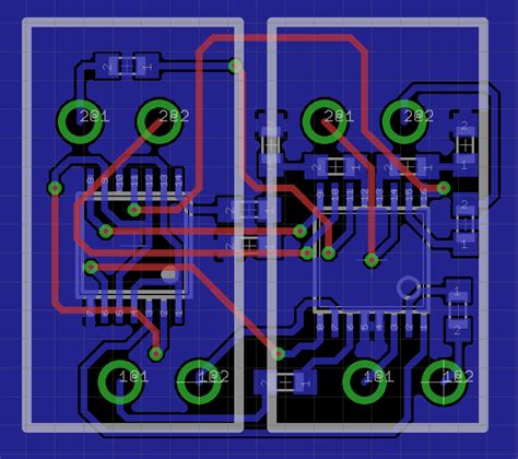
Routing Traces
Once the components are placed, the next step is to route the traces that connect them. Trace routing is a critical aspect of PCB layout design, as it directly impacts signal integrity, EMI, and manufacturability.
Trace Width and Spacing
The width of a trace determines its current-carrying capacity and resistance. Wider traces can handle higher currents and have lower resistance, but they also take up more space on the PCB. The spacing between traces is equally important, as it affects the board’s ability to withstand voltage differences and influences crosstalk between signals.
When selecting trace widths and spacings, consider the following factors:
- Current requirements: Use wider traces for high-current paths, such as power supply lines.
- Signal integrity: Ensure that traces carrying high-speed or sensitive signals are adequately spaced to minimize crosstalk and maintain signal integrity.
- Manufacturing constraints: Adhere to the minimum trace width and spacing requirements specified by your PCB manufacturer to ensure reliable fabrication.
Via Placement
Vias are small holes drilled through the PCB layers to connect traces on different layers. They are essential for multi-layer PCBs and can also be used to route traces on single-layer boards. When placing vias, consider the following guidelines:
- Via size: Use the smallest via size that meets your current and manufacturing requirements to minimize board space and improve signal integrity.
- Via location: Place vias strategically to minimize trace lengths and avoid interfering with component placement.
- Via-in-pad: In some cases, placing a via directly on a component pad can save space and simplify routing. However, ensure that your manufacturer supports this technique and that it does not compromise solderability.
Ground Planes and Power Distribution
Proper grounding and power distribution are essential for PCB performance and reliability. A ground plane is a large copper area on one or more layers of the PCB that provides a low-impedance return path for currents. Power planes, similarly, distribute power to components across the board.
When designing ground and power planes, keep these tips in mind:
- Solid planes: Use solid planes instead of gridded or hatched patterns to minimize impedance and improve EMI shielding.
- Split planes: If your design includes both analog and digital circuits, consider splitting the ground and power planes to minimize noise coupling between the two domains.
- Decoupling capacitors: Place decoupling capacitors close to the power pins of ICs to reduce high-frequency noise and ensure stable power delivery.

Signal Integrity and EMI Considerations
Maintaining signal integrity and minimizing electromagnetic interference (EMI) are critical aspects of PCB layout design. Poor signal integrity can lead to data corruption, while excessive EMI can cause interference with other devices and violate regulatory requirements.
Crosstalk and Impedance Matching
Crosstalk occurs when signals on adjacent traces interfere with each other due to electromagnetic coupling. To minimize crosstalk, follow these guidelines:
- Trace spacing: Increase the spacing between traces carrying sensitive or high-speed signals.
- Shielding: Use grounded traces or planes between sensitive signals to provide shielding and reduce crosstalk.
- Impedance matching: Ensure that the impedance of traces matches the impedance of the source and load to minimize reflections and signal distortion.
EMI Reduction Techniques
To reduce EMI, consider the following techniques:
- Proper grounding: Use a solid ground plane and provide low-impedance return paths for high-frequency currents.
- Shielding: Incorporate shielding measures, such as grounded copper pours or metal enclosures, to contain EMI.
- Filters: Use filters, such as ferrite beads or LC filters, to suppress high-frequency noise on power and signal lines.
- Spread-spectrum clocking: Employ spread-spectrum clocking techniques to reduce the peak energy of clock signals and minimize EMI.
PCB Manufacturing Considerations
When designing your PCB layout, it is essential to keep in mind the capabilities and limitations of your chosen PCB manufacturer. This will help ensure that your design can be successfully fabricated and assembled.
Design Rule Checking (DRC)
Most PCB design software includes a Design Rule Checking (DRC) feature that helps identify and resolve layout issues based on a set of predefined rules. These rules encompass various aspects of PCB design, such as:
- Minimum trace width and spacing
- Minimum via size and drill diameter
- Minimum clearance between components and traces
- Solder mask and silkscreen guidelines
By running DRC checks regularly during the layout process, you can catch and fix potential problems early, saving time and effort in the long run.
Panelization and Assembly
If your design includes multiple small PCBs, consider panelizing them to reduce manufacturing costs and streamline assembly. Panelization involves arranging multiple PCBs on a single panel, with breakaway tabs or scoring lines to separate them after fabrication.
When panelizing your design, keep these factors in mind:
- Panel size: Ensure that your panel size is compatible with your manufacturer’s equipment and processes.
- Tooling holes: Include tooling holes in the panel to aid in registration and alignment during fabrication and assembly.
- Assembly notes: Provide clear and concise assembly notes, including component orientations, special handling requirements, and test points.
Best Practices for PCB Layout Design
To create effective and efficient PCB layouts, follow these best practices:
-
Start with a well-organized schematic: A clean and well-structured schematic is the foundation of a successful PCB layout.
-
Plan your component placement: Carefully consider component placement to optimize signal paths, minimize crosstalk, and ensure proper thermal management.
-
Use a consistent grid: Align components and traces to a consistent grid to improve readability and manufacturability.
-
Keep traces short and direct: Minimize trace lengths to reduce resistance, inductance, and signal degradation.
-
Avoid sharp corners: Use 45-degree angles or curved traces instead of 90-degree corners to reduce signal reflections and improve manufacturability.
-
Provide adequate clearances: Ensure that there is sufficient clearance between components, traces, and board edges to accommodate manufacturing tolerances and prevent short circuits.
-
Use copper pours: Fill unused areas of the PCB with copper pours connected to ground to improve EMI shielding and reduce impedance.
-
Incorporate test points: Include test points in your layout to facilitate debugging and quality control during manufacturing and assembly.
-
Document your design: Provide clear and comprehensive documentation, including a bill of materials (BOM), assembly drawings, and any special instructions, to ensure smooth communication with your manufacturer.
-
Collaborate with your manufacturer: Work closely with your PCB manufacturer to ensure that your design meets their capabilities and guidelines, and be open to their feedback and suggestions for improvement.
FAQ
- What software is used for PCB layout design?
Several software packages are commonly used for PCB layout design, including: - Autodesk Eagle
- KiCad
- Altium Designer
- Cadence OrCAD
-
Mentor Graphics PADS
-
How do I choose the right PCB manufacturer for my project?
When selecting a PCB manufacturer, consider the following factors: - Experience and expertise in your specific industry or application
- Manufacturing capabilities and technology
- Quality control and certifications (e.g., ISO, UL, RoHS)
- Lead times and pricing
-
Customer support and communication
Research potential manufacturers and request quotes and samples to compare their services and capabilities. -
What are the most common PCB assembly methods?
The two main PCB assembly methods are: - Through-hole assembly (THA): Components with leads are inserted through holes drilled in the PCB and soldered on the opposite side.
-
Surface-mount assembly (SMA): Components are placed directly on the surface of the PCB and soldered using a reflow oven or wave soldering process.
-
How can I reduce the cost of my PCB design?
To reduce the cost of your PCB design, consider the following strategies: - Minimize the board size and layer count
- Use standard component packages and footprints
- Avoid unnecessary features, such as custom silkscreen or non-standard board shapes
- Opt for larger minimum trace widths and spacings to improve manufacturability
-
Panelize multiple designs to take advantage of volume discounts
-
What are the typical lead times for PCB fabrication and assembly?
Lead times for PCB fabrication and assembly can vary depending on the complexity of your design, the manufacturer’s workload, and the shipping method. Typical lead times range from 1-2 weeks for standard designs to 4-6 weeks for more complex or customized projects. Expedited services may be available for an additional cost.
| PCB Characteristic | Typical Value Range |
|---|---|
| Trace Width | 0.1 mm – 0.5 mm |
| Trace Spacing | 0.1 mm – 0.5 mm |
| Via Diameter | 0.3 mm – 0.8 mm |
| Via Drill Diameter | 0.2 mm – 0.6 mm |
| Minimum Hole Size | 0.3 mm – 0.8 mm |
| Copper Thickness | 0.5 oz – 2 oz |
| Board Thickness | 0.4 mm – 3.2 mm |
Conclusion
PCB layout design is a complex and iterative process that requires a combination of technical knowledge, attention to detail, and creative problem-solving. By understanding the basics of PCB design, planning your layout carefully, and following best practices and manufacturing guidelines, you can create reliable, high-performance PCBs that meet your project’s requirements.
As you gain experience and tackle more advanced designs, continue to learn from your successes and failures, stay up-to-date with the latest industry trends and technologies, and collaborate closely with your PCB manufacturer to ensure the best possible results.


Leave a Reply