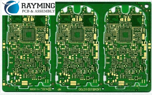
Choosing the right printed circuit board (PCB) stackup is critical for ensuring your PCB design meets your electrical, thermal, and mechanical requirements. The stackup refers to the sequence and thicknesses of the conductive copper and insulating dielectric layers in your PCB. Selecting an optimal stackup requires balancing many factors like signal integrity, EMI control, thermal dissipation, manufacturability, and cost. This article provides a step-by-step guide to choosing the best stackup for your next PCB design.
Key Factors to Consider
When selecting a PCB stackup, the most important factors to consider are:
Signal Integrity
Your stackup must enable clear transmission of signals between chips, connectors, and other components on your board. Trace impedances must match component requirements to avoid signal reflection and distortion. Your stackup design impacts options for routing critical signals on inner layers.
EMI Control
A good stackup minimizes electromagnetic interference (EMI) radiated from your device. Strategies like buried capacitance planes, shielding layers, and differential signaling require specific stackup configurations.
Thermal Management
The stackup must enable adequate heat dissipation from hot components through inner ground planes and thermal vias to outer layers. More dielectric layers tend to insulate while thicker copper layers spread heat better.
Manufacturability
Your PCB manufacturer has constraints around the number of layers, materials, thicknesses, and tolerances they support. Your stackup must align with their capabilities to avoid fab issues.
Cost
More layers and thicker copper increase costs. Balance signal integrity and thermal needs with budget considerations when selecting layer count.
Steps to Selecting Your PCB Stackup
Follow these steps to design the optimal stackup for your next PCB:
1. Define Your Layer Count
Consider the minimum number of layers needed for routing your required component placement and traces. Here are typical layer counts:
- 2-layer: Simple, low component density boards
- 4-layer: Most common for cost/complexity balance
- 6-layer or more: Complex boards with high speed, RF, or flex requirements
Also factor in any shielding, buried capacitance, or impedance control layers needed beyond basic signal routing.
2. Select Your Dielectric Materials
FR-4 glass epoxy is the most common, cost-effective PCB dielectric. High-speed boards may use low-loss materials like FR-408, Rogers, or polyimides. Refer to your PCB manufacturer’s material offerings and properties.
Consider factors like dielectric constant, loss tangent, thermal conductivity, Tg, Z-axis CTE, and moisture absorption.
3. Define Your Copper Layer Thicknesses
Copper thickness impacts cost and electrical/thermal performance. Standard thicknesses are:
- 1 oz (35 μm) – Common for outer layers
- 2 oz (70 μm) – Used for high current inner layers
- 1/2 oz (17 μm) – Economical for inner layers
- 1/4 oz (8 μm) – Only for controlled impedance layers
Thicker copper spreads heat better while thinner copper reduces costs.
4. Create Your Layer Sequence
Arrange layers in a sequence that meets your design requirements. Some guidelines:
- Place ground planes adjacent to critical signal layers for shielding.
- Ensure power and ground planes are close to high-power components.
- Put the thickest copper layers in the center if needed for heat spreading.
- Ensure any shielding, buried capacitance, or controlled impedance layers are properly positioned.
Here is an example 6-layer stackup:
| Layer | Type | Thickness |
|---|---|---|
| 1 (top) | Signal | 1 oz |
| 2 | Ground | 1 oz |
| 3 | Power | 2 oz |
| 4 | Ground | 1 oz |
| 5 | Signal | 1 oz |
| 6 | Signal (bottom) | 1 oz |
5. Perform Simulation and Review
Use stackup planning tools from your PCB design software to model your preliminary stackup. Simulate signal transmission, EMI, and thermal performance. Refine the stackup as needed to resolve any issues identified.
6. Confirm Manufacturability
Work with your PCB manufacturer early in the design process to confirm that your planned stackup aligns with their capabilities and recommendations. Make any adjustments to ensure manufacturability.
Additional Stackup Design Considerations
Beyond the core steps outlined above, also consider the following stackup design factors:
- Number and size of drill holes needed for vias
- Split power planes to isolate noise-sensitive supplies
- Allow for fine pitch component lead separation
- Enable RF trace impedance control as needed
- Incorporate buried and blind vias where beneficial
- Include provisions for conformal coatings and test points
When to Engage a PCB Layout Expert
For complex designs with tight signal integrity, EMI, thermal, or manufacturability requirements, engage an expert PCB layout engineer to design your stackup. Their experience with different materials, sequencing, and modeling techniques will ensure you get an optimized stackup.
This upfront investment will pay dividends by enabling successful PCB fabrication the first time and avoiding costly respins.
Conclusion
- Begin by defining the necessary layer count for your design complexity.
- Choose appropriate dielectric materials suited for your application.
- Select copper weights to balance cost, thermal, and electrical needs.
- Sequence layers to prioritize signal integrity, shielding, and heat flow.
- Verify performance through modeling and simulations.
- Confirm manufacturability with your PCB fabricator.
Carefully planning your PCB stackup is time well spent to avoid performance issues, delays, and unnecessary cost. Leverage available stackup design expertise and manufacturing guidance when possible. Applying the guidelines in this article will lead to successful first-pass PCB fabrication.
Frequently Asked Questions
What is the most common PCB stackup?
The most common PCB stackup is a 4-layer board using standard FR-4 dielectric material. This consists of a top and bottom signal layer separated by a power and ground plane. The 4-layer stackup provides a good balance of routability, signal integrity, EMI control, and cost for many designs.
How do I know if I need more than 4 PCB layers?
You will likely need more than 4 layers if you have dense component placement that won’t route properly on 2 signal layers, complex power distribution needs, high-speed signals requiring impedance control, or RF signals needing shielding. High pin-count BGAs, fine pitch QFNs, DDR3 routing, and RF circuits often require 6 layers or more.
What dielectric materials offer the best high-speed performance?
Materials like FR-408, Rogers 4350, and some polyimides offer superior electrical performance for high-speed or RF PCBs compared to standard FR-4. They have tightly controlled dielectric constants, lower loss tangents, and consistent properties. This enables better impedance control and signal integrity at higher frequencies.
How do I decide on copper weights for each layer?
Use thicker 2 oz copper for high current power distribution layers. Use standard 1 oz copper for signal layers and perhaps a thin 0.5 oz copper for inner ground planes. Only use ultra-thin 0.25 oz copper for tightly controlled impedance layers when the thinnest dielectric spacing is needed. Heavier copper layers improve thermal heat spreading.
What is a buried capacitance layer and when should I use one?
Buried capacitance layers use a thin high dielectric constant material laminated between two copper planes to create embedded capacitance within the PCB. This provides decoupling capacitance near ICs to reduce power distribution noise. It requires careful stackup design and modeling for proper performance.
How can I ensure my stackup is manufacturable?
Discuss layer count, materials selected, copper weights, and any tight tolerances with your PCB manufacturer early in your design process. Confirm your planned stackup aligns with their fabrication capabilities and make adjustments as needed. Get their recommendations to avoid any manufacturability issues.


Leave a Reply