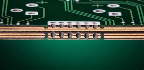
What is a High Current PCB?
A high current PCB, also known as a power PCB or heavy copper PCB, is a printed circuit board designed to handle high levels of electrical current. These PCBs are used in power electronics applications such as power supplies, motor controls, inverters, and battery management systems.
High current PCBs differ from standard PCBs in several ways:
- They use thicker copper traces and planes to handle the higher current levels
- They require special design considerations for thermal management to dissipate the heat generated by the high currents
- They may use different materials and manufacturing processes compared to standard PCBs
The key characteristics of a high current PCB are:
| Characteristic | Description |
|---|---|
| High Current Handling | Able to handle currents of 1A or more per trace |
| Thick Copper | Uses copper thicknesses of 2oz (70μm) or greater |
| Thermal Management | Incorporates features for heat dissipation such as large copper areas, thermal vias, and heatsinks |
| High Voltage | May need to withstand voltages over 100V |
| Rugged Construction | Uses strong substrate materials and reinforcements to withstand mechanical stresses |
Designing a high current PCB requires careful consideration of the electrical, thermal, and mechanical requirements of the application. In the following sections, we will discuss the key design and optimization techniques for creating a perfect high current PCB.
Choosing the Right Copper Thickness
One of the most critical aspects of high current PCB design is selecting the appropriate copper thickness for the traces and planes. The copper thickness determines the current carrying capacity of the traces and the ability to dissipate heat.
The standard copper thicknesses used in PCBs are:
| Copper Weight | Thickness (μm) | Typical Current Capacity (A/mm) |
|---|---|---|
| 0.5 oz | 18 | 1.4 |
| 1 oz | 35 | 2.8 |
| 2 oz | 70 | 5.6 |
| 3 oz | 105 | 8.4 |
| 4 oz | 140 | 11.2 |
For high current applications, it is recommended to use a minimum of 2oz (70μm) copper. However, for very high currents, even thicker copper such as 3oz or 4oz may be necessary.
When selecting the copper thickness, it is important to consider not only the current carrying capacity but also the manufacturability and cost of the PCB. Thicker copper requires more etching time and may increase the cost of the PCB. It can also make the PCB less flexible and more prone to warping.
One way to optimize the copper thickness is to use different thicknesses for different layers of the PCB. For example, the inner layers that carry high currents can use thicker copper, while the outer layers used for signal routing can use thinner copper. This hybrid stackup allows for a balance of current capacity and manufacturability.

Optimizing Trace Widths and Clearances
In addition to copper thickness, the width of the traces and the clearances between them also play a crucial role in high current PCB design.
The trace width determines the resistance of the trace and thus the amount of power dissipation. Wider traces have lower resistance and can carry more current without overheating. The IPC-2221 standard provides guidelines for minimum trace widths based on the copper thickness and the expected current.
For example, for a 2oz copper trace carrying 5A of current, the minimum recommended trace width is 120 mils (3mm). However, it is often desirable to use even wider traces to provide a margin of safety and to reduce the temperature rise.
The clearance between traces is also important for high current PCBs. Sufficient clearance is needed to prevent arcing and short circuits, especially in high voltage applications. The IPC-2221 standard provides guidelines for minimum clearances based on the voltage and the pollution degree of the environment.
For example, for a PCB operating at 300V in a pollution degree 2 environment, the minimum clearance between traces is 1.5mm.
When routing high current traces, it is important to keep them as short and straight as possible to minimize the resistance and inductance. Avoid sharp corners and use gentle curves instead. Also, keep high current traces away from sensitive signals to prevent interference.

Using Copper Pours and Planes
Another effective technique for optimizing high current PCBs is to use copper pours and planes. Instead of using individual traces to carry the current, a large area of copper is used to provide a low-resistance path.
Copper pours are typically used on the outer layers of the PCB to provide a low-impedance ground or power connection. They also help to dissipate heat and provide shielding against electromagnetic interference (EMI).
Copper planes are used on the inner layers of the PCB to provide a low-resistance path for power distribution. They are typically used in conjunction with power and ground planes to create a low-impedance power distribution network (PDN).
When using copper pours and planes, it is important to consider the current density and the thermal requirements. The current density should not exceed the maximum allowable value for the copper thickness used. For example, for 2oz copper, the maximum current density is typically around 20A/mm².
To optimize the thermal performance of copper pours and planes, it is important to use thermal relief connections to the traces and components. Thermal reliefs are small traces that connect the component pads to the copper pour, allowing for some thermal isolation. Without thermal reliefs, the large copper area can act as a heat sink and cause soldering difficulties.

Thermal Management Techniques
Thermal management is a critical aspect of high current PCB design. The high currents flowing through the traces and components generate significant amounts of heat that must be dissipated to prevent overheating and failure.
There are several techniques that can be used to optimize the thermal performance of high current PCBs:
Using Thermal Vias
Thermal vias are small holes drilled through the PCB that are filled with copper. They provide a low-resistance thermal path from the components to the other side of the PCB, where the heat can be dissipated by heatsinks or cooling fans.
Thermal vias are typically placed under high-power components such as MOSFETs, diodes, and resistors. They should be placed as close to the component as possible to minimize the thermal resistance.
When using thermal vias, it is important to consider the drilling and plating capabilities of the PCB manufacturer. The vias should be large enough to provide sufficient thermal conductivity but small enough to be reliably drilled and plated.
Using Heatsinks
Heatsinks are metal structures that are attached to the PCB to provide additional cooling. They work by increasing the surface area available for heat dissipation and by providing a low-resistance thermal path to the ambient air.
Heatsinks can be attached to the PCB using thermal adhesive, mechanical fasteners, or soldering. They are typically made of aluminum or copper and can be customized to fit the specific requirements of the application.
When selecting a heatsink, it is important to consider the thermal resistance, the size, and the cost. The thermal resistance should be low enough to provide sufficient cooling, while the size should be compatible with the available space on the PCB. The cost should be balanced against the performance requirements and the production volume.
Using Cooling Fans
Cooling fans are another option for thermal management in high current PCBs. They work by forcing air over the PCB and the components, increasing the convective heat transfer.
Cooling fans can be mounted directly on the PCB or can be part of a separate enclosure. They are typically controlled by temperature sensors that turn the fan on when the temperature exceeds a certain threshold.
When using cooling fans, it is important to consider the airflow direction, the noise level, and the power consumption. The airflow should be directed over the hottest components and should not be obstructed by other components or structures. The noise level should be acceptable for the application, and the power consumption should be compatible with the available power budget.
Materials Selection
The materials used in high current PCBs also play a critical role in their performance and reliability. The substrate material, the copper foil, and the solder mask all have an impact on the electrical, thermal, and mechanical properties of the PCB.
The most common substrate material for high current PCBs is FR-4, which is a glass-reinforced epoxy laminate. FR-4 has good electrical and mechanical properties and is compatible with standard PCB manufacturing processes. However, for high-temperature applications or applications requiring higher thermal conductivity, other materials such as aluminum, ceramic, or metal-core PCBs may be used.
The copper foil used in high current PCBs should be of high quality and purity to minimize the resistance and the losses. The copper foil should also have good adhesion to the substrate material to prevent delamination and cracking.
The solder mask used in high current PCBs should be able to withstand the high temperatures and the mechanical stresses associated with the application. It should also provide good electrical insulation and protection against environmental factors such as moisture and chemicals.
Testing and Verification
Once the high current PCB is designed and manufactured, it is important to test and verify its performance and reliability. This includes both electrical and thermal testing to ensure that the PCB meets the specified requirements.
Electrical testing typically includes resistance measurements, continuity tests, and high-potential (hipot) tests to verify the integrity of the traces and the insulation. It may also include functional tests to verify the operation of the circuits and the components.
Thermal testing typically includes temperature measurements using thermocouples or infrared cameras to verify that the PCB does not exceed the maximum allowable temperatures. It may also include power cycling tests to simulate the expected operating conditions and to verify the long-term reliability of the PCB.
FAQs
What is the difference between a high current PCB and a standard PCB?
A high current PCB is designed to handle higher levels of electrical current compared to a standard PCB. It uses thicker copper traces and planes, special thermal management techniques, and rugged construction to handle the high currents and the associated heat generation.
What is the minimum copper thickness for a high current PCB?
For high current applications, it is recommended to use a minimum of 2oz (70μm) copper. However, for very high currents, even thicker copper such as 3oz or 4oz may be necessary.
What is the purpose of thermal vias in a high current PCB?
Thermal vias are small holes drilled through the PCB that are filled with copper. They provide a low-resistance thermal path from the components to the other side of the PCB, where the heat can be dissipated by heatsinks or cooling fans.
What materials are used for high current PCBs?
The most common substrate material for high current PCBs is FR-4, which is a glass-reinforced epoxy laminate. However, for high-temperature applications or applications requiring higher thermal conductivity, other materials such as aluminum, ceramic, or metal-core PCBs may be used.
What tests are performed on high current PCBs?
High current PCBs undergo both electrical and thermal testing to verify their performance and reliability. Electrical testing includes resistance measurements, continuity tests, and high-potential (hipot) tests, while thermal testing includes temperature measurements and power cycling tests.
Conclusion
Designing and optimizing high current PCBs requires careful consideration of the electrical, thermal, and mechanical requirements of the application. By using the right copper thickness, optimizing trace widths and clearances, using copper pours and planes, and implementing effective thermal management techniques, it is possible to create a perfect high current PCB that meets the performance and reliability requirements of the application. Proper materials selection and thorough testing and verification are also critical to ensuring the success of the project.


Leave a Reply