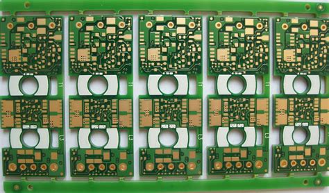
What Is An Extreme Copper PCB?
An Extreme Copper PCB, also known as a Heavy Copper PCB, is a printed circuit board that uses thicker copper traces than standard PCBs. While a typical PCB might have copper traces with a thickness of 1 oz (35 μm), an Extreme Copper PCB can have traces ranging from 4 oz (140 μm) to 20 oz (700 μm) or even higher. This increased copper thickness provides several benefits, especially in high-temperature and extreme environments.
Benefits Of Extreme Copper PCBs
- Enhanced Current Carrying Capacity
- Improved Heat Dissipation
- Increased Mechanical Strength
- Better Signal Integrity
| Copper Weight (oz) | Thickness (μm) | Current Carrying Capacity (A) |
|---|---|---|
| 1 | 35 | 5 |
| 2 | 70 | 10 |
| 4 | 140 | 20 |
| 6 | 210 | 30 |
| 10 | 350 | 50 |
| 20 | 700 | 100 |
Applications Of Extreme Copper PCBs In High-Temperature Environments
Automotive Industry
In the automotive industry, Extreme Copper PCBs are used in various high-temperature applications, such as:
- Engine Control Units (ECUs)
- Transmission Control Modules (TCMs)
- Brake Control Modules (BCMs)
- Exhaust Gas Recirculation (EGR) Systems
These PCBs must withstand temperatures ranging from -40°C to +150°C, as well as vibrations and thermal cycling. The thick copper traces of Extreme Copper PCBs help to dissipate heat more effectively, ensuring reliable operation in these harsh conditions.
Aerospace And Defense
Extreme Copper PCBs are essential in aerospace and defense applications, where high temperatures and extreme environments are common. Some examples include:
- Radar Systems
- Satellite Communications
- Avionics
- Missile Guidance Systems
In these applications, PCBs may be exposed to temperatures exceeding 200°C, as well as high levels of radiation and electromagnetic interference (EMI). The increased copper thickness of Extreme Copper PCBs provides better shielding against EMI and improves signal integrity in these demanding environments.
Industrial Equipment
Industrial equipment, such as power electronics and motor drives, often requires Extreme Copper PCBs to handle high currents and temperatures. Some specific applications include:
- Welding Equipment
- Induction Heating Systems
- High-Power Inverters
- Motor Control Units
These PCBs must be able to withstand temperatures up to 150°C and handle currents exceeding 100 A. The enhanced current carrying capacity and improved heat dissipation properties of Extreme Copper PCBs make them ideal for these industrial applications.

Design Considerations For Extreme Copper PCBs
Thermal Management
Proper thermal management is crucial when designing Extreme Copper PCBs for high-temperature environments. Some key considerations include:
- Copper Thickness: Selecting the appropriate copper thickness based on the expected current and temperature requirements.
- Thermal Vias: Incorporating thermal vias to transfer heat from the components to the copper layers and eventually to the heat sink.
- Heat Sinks: Using heat sinks and other cooling solutions to dissipate heat more effectively.
- Component Placement: Placing temperature-sensitive components away from high-heat sources and providing adequate spacing for heat dissipation.
Material Selection
Choosing the right materials is essential for Extreme Copper PCBs in high-temperature environments. Some important factors to consider include:
- Base Material: Using high-temperature base materials, such as polyimide (PI) or high-Tg FR-4, which can withstand temperatures up to 200°C.
- Solder Mask: Selecting a high-temperature solder mask that can withstand the expected operating temperatures without cracking or peeling.
- Surface Finish: Choosing a surface finish that can withstand high temperatures and provide good solderability, such as Electroless Nickel Immersion Gold (ENIG) or Electroless Nickel Electroless Palladium Immersion Gold (ENEPIG).
Manufacturing Challenges
Manufacturing Extreme Copper PCBs for high-temperature environments presents several challenges, including:
- Plating: Achieving even copper plating across the board can be difficult with thicker copper traces. Specialized plating processes, such as pulse plating or reverse pulse plating, may be required.
- Etching: Etching thicker copper traces requires longer etching times and more precise control to achieve the desired trace widths and spacing.
- Drilling: Drilling through thicker copper layers can cause drill bits to wear out more quickly and may require specialized drilling techniques, such as stepped drilling or high-speed drilling.
- Lamination: Ensuring proper lamination of the layers can be challenging with thicker copper, as the increased copper weight can cause shifting or misalignment during the lamination process.

Testing And Qualification Of Extreme Copper PCBs
To ensure the reliability and performance of Extreme Copper PCBs in high-temperature environments, rigorous testing and qualification processes are necessary. Some common tests include:
- Thermal Cycling: Exposing the PCB to repeated cycles of high and low temperatures to simulate real-world operating conditions and assess the board’s ability to withstand thermal stress.
- Thermal Shock: Subjecting the PCB to rapid temperature changes to evaluate its resistance to thermal shock and identify potential weaknesses in the design or manufacturing process.
- Burn-In Testing: Operating the PCB at elevated temperatures for an extended period to identify any early failures or defects that may not be apparent under normal operating conditions.
- Vibration And Shock Testing: Exposing the PCB to mechanical stresses, such as vibration and shock, to ensure it can withstand the rigors of the intended application.
- Electrical Testing: Conducting various electrical tests, such as continuity, insulation resistance, and high-potential (hipot) testing, to verify the PCB’s electrical performance and integrity.

Future Trends In Extreme Copper PCBs For High-Temperature Environments
As technology advances and the demand for reliable electronics in extreme environments grows, several trends are emerging in the development of Extreme Copper PCBs:
- Advanced Materials: Researchers are exploring new base materials, such as ceramic substrates and metal-core PCBs, that can withstand even higher temperatures and provide better thermal conductivity.
- Embedded Components: Integrating passive components, such as resistors and capacitors, directly into the PCB substrate can help reduce the board’s size and improve its thermal performance.
- 3D Printing: Additive manufacturing techniques, such as 3D printing, are being investigated as a means to create complex copper structures and improve heat dissipation in Extreme Copper PCBs.
- Simulation And Modeling: Advanced simulation and modeling tools are being developed to better predict the thermal and mechanical behavior of Extreme Copper PCBs in high-temperature environments, allowing for more optimized designs and reduced testing time.
As these trends continue to evolve, Extreme Copper PCBs will become even more capable of withstanding the challenges posed by high-temperature and extreme environments, enabling the development of more advanced and reliable electronic systems.
Frequently Asked Questions (FAQ)
1. What is the difference between a standard PCB and an Extreme Copper PCB?
The main difference between a standard PCB and an Extreme Copper PCB is the thickness of the copper traces. While a standard PCB typically has copper traces with a thickness of 1 oz (35 μm), an Extreme Copper PCB can have traces ranging from 4 oz (140 μm) to 20 oz (700 μm) or even higher. This increased copper thickness provides several benefits, such as enhanced current carrying capacity, improved heat dissipation, and increased mechanical strength.
2. What are some common applications for Extreme Copper PCBs in high-temperature environments?
Extreme Copper PCBs are commonly used in various high-temperature applications, including:
- Automotive: Engine Control Units (ECUs), Transmission Control Modules (TCMs), and Exhaust Gas Recirculation (EGR) Systems.
- Aerospace and Defense: Radar Systems, Satellite Communications, Avionics, and Missile Guidance Systems.
- Industrial Equipment: Welding Equipment, Induction Heating Systems, High-Power Inverters, and Motor Control Units.
3. What are some key design considerations when creating an Extreme Copper PCB for high-temperature environments?
When designing an Extreme Copper PCB for high-temperature environments, some key considerations include:
- Thermal Management: Selecting the appropriate copper thickness, incorporating thermal vias, using heat sinks, and proper component placement.
- Material Selection: Choosing high-temperature base materials, solder masks, and surface finishes that can withstand the expected operating temperatures.
- Manufacturing Challenges: Addressing issues related to plating, etching, drilling, and lamination of thicker copper traces.
4. What types of testing are performed on Extreme Copper PCBs to ensure their reliability in high-temperature environments?
To ensure the reliability and performance of Extreme Copper PCBs in high-temperature environments, several tests are performed, including:
- Thermal Cycling: Exposing the PCB to repeated cycles of high and low temperatures.
- Thermal Shock: Subjecting the PCB to rapid temperature changes.
- Burn-In Testing: Operating the PCB at elevated temperatures for an extended period.
- Vibration and Shock Testing: Exposing the PCB to mechanical stresses.
- Electrical Testing: Conducting continuity, insulation resistance, and high-potential (hipot) testing.
5. What are some future trends in the development of Extreme Copper PCBs for high-temperature environments?
Some future trends in the development of Extreme Copper PCBs for high-temperature environments include:
- Advanced Materials: Exploring new base materials, such as ceramic substrates and metal-core PCBs.
- Embedded Components: Integrating passive components directly into the PCB substrate.
- 3D Printing: Using additive manufacturing techniques to create complex copper structures and improve heat dissipation.
- Simulation and Modeling: Developing advanced tools to better predict the thermal and mechanical behavior of Extreme Copper PCBs.
As technology continues to advance, Extreme Copper PCBs will become increasingly capable of withstanding the challenges posed by high-temperature and extreme environments, enabling the development of more advanced and reliable electronic systems.


Leave a Reply