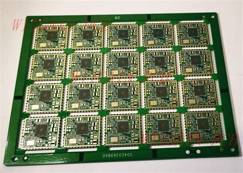
What is an HDI PCB?
An HDI PCB is a printed circuit board that features higher wiring density per unit area than conventional PCBs. This is achieved through the use of smaller vias, finer trace widths, and tighter spacing between components. HDI PCBs can have multiple layers, with microvias connecting the layers, enabling complex routing and enhanced functionality in a compact form factor.
Benefits of HDI PCBs
-
Miniaturization: HDI technology allows for the creation of smaller, more compact PCBs, making them ideal for applications where space is limited, such as smartphones, wearables, and IoT devices.
-
Increased Functionality: With the ability to accommodate more components and complex routing, HDI PCBs enable the integration of more features and functions into a single board.
-
Improved Signal Integrity: The reduced trace lengths and smaller vias in HDI PCBs minimize signal loss and distortion, resulting in better signal integrity and overall performance.
-
Cost-Effective: Although the initial manufacturing costs may be higher, HDI PCBs often lead to cost savings in the long run due to reduced assembly time, fewer components, and improved reliability.
HDI PCB Design Considerations
Designing an HDI PCB requires careful consideration of various factors to ensure optimal performance and manufacturability. Here are some key design considerations:
Layer Stack-up
The layer stack-up is a critical aspect of HDI PCB design. It determines the number of layers, the arrangement of signal, power, and ground planes, and the placement of microvias. A well-designed stack-up ensures proper signal integrity, power distribution, and thermal management.
| Layer | Material | Thickness (mm) |
|---|---|---|
| Top Layer | Copper | 0.035 |
| Dielectric 1 | FR-4 | 0.1 |
| Inner Layer 1 | Copper | 0.018 |
| Dielectric 2 | FR-4 | 0.1 |
| Inner Layer 2 | Copper | 0.018 |
| Dielectric 3 | FR-4 | 0.1 |
| Bottom Layer | Copper | 0.035 |
Via Types and Sizes
HDI PCBs utilize various types of vias, including through-hole vias, blind vias, and buried vias. The choice of via type depends on the layer stack-up and the specific design requirements. Microvias, with diameters typically less than 0.15mm, are commonly used in HDI designs to connect the outer layers to the inner layers.
| Via Type | Diameter (mm) | Depth (mm) |
|---|---|---|
| Through-hole | 0.3 | 1.6 |
| Blind | 0.2 | 0.4 |
| Buried | 0.1 | 0.2 |
Trace Width and Spacing
To achieve higher wiring density, HDI PCBs employ finer trace widths and tighter spacing between traces. The minimum trace width and spacing depend on the PCB manufacturer’s capabilities and the desired impedance control. Typical values range from 0.075mm to 0.1mm for trace width and spacing.
Component Selection and Placement
Component selection and placement play a crucial role in HDI PCB design. Smaller package sizes, such as chip-scale packages (CSPs) and ball grid arrays (BGAs), are commonly used to minimize the board real estate. Careful consideration should be given to component placement to ensure optimal routing, signal integrity, and thermal management.

HDI PCB Manufacturing Process
The manufacturing process for HDI PCBs involves several specialized techniques to achieve the required precision and reliability. Here are the key steps involved:
-
Drilling: High-precision drilling machines are used to create the various types of vias, including through-hole, blind, and buried vias.
-
Plating: The drilled holes are plated with copper to establish electrical connections between layers. Specialized plating techniques, such as via-in-pad plating, are employed to achieve reliable connections.
-
Patterning: The copper layers are patterned using photolithography and etching processes to create the desired trace patterns and component pads.
-
Lamination: The individual layers are laminated together using high-pressure and temperature to form a solid, multi-layer PCB.
-
Surface Finish: A suitable surface finish, such as ENIG (Electroless Nickel Immersion Gold) or ENEPIG (Electroless Nickel Electroless Palladium Immersion Gold), is applied to protect the exposed copper and enhance solderability.

Best Practices for HDI PCB Design and Manufacturing
To ensure the success of your HDI PCB project, consider the following best practices:
-
Collaborate with your PCB manufacturer: Engage with your PCB manufacturer early in the design process to discuss your requirements, design constraints, and manufacturing capabilities. Their expertise can help optimize your design for manufacturability and reliability.
-
Follow design guidelines: Adhere to the recommended design guidelines provided by your PCB manufacturer, including minimum trace widths, spacing, via sizes, and drill hole tolerances. This ensures that your design is compatible with their manufacturing processes.
-
Perform thorough design reviews: Conduct comprehensive design reviews at various stages of the design process to catch and rectify any potential issues early on. Use design rule checks (DRCs) and simulations to verify the integrity of your design.
-
Consider signal integrity: Pay close attention to signal integrity considerations, such as impedance control, crosstalk, and EMI/EMC. Use appropriate design techniques, such as proper grounding, shielding, and differential pair routing, to mitigate signal integrity issues.
-
Plan for testing and inspection: Incorporate testability features into your HDI PCB design, such as test points and boundary scan chains, to facilitate efficient testing and debugging. Work with your manufacturer to establish a robust quality control and inspection plan.

Frequently Asked Questions (FAQ)
-
What is the minimum via size achievable in HDI PCBs?
The minimum via size in HDI PCBs depends on the manufacturer’s capabilities. Typically, microvias with diameters as small as 0.1mm can be achieved. -
Can HDI PCBs be used for high-power applications?
Yes, HDI PCBs can be designed for high-power applications by incorporating appropriate power planes, thermal management techniques, and selecting suitable materials with high thermal conductivity. -
How do HDI PCBs compare to traditional PCBs in terms of cost?
The initial manufacturing cost of HDI PCBs may be higher due to the specialized processes and materials involved. However, the overall cost-effectiveness can be realized through reduced assembly time, fewer components, and improved reliability. -
What are the common materials used in HDI PCBs?
HDI PCBs commonly use high-performance materials such as FR-4, polyimide, and Rogers materials. The choice of material depends on the specific requirements of the application, such as thermal stability, dielectric constant, and loss tangent. -
How can I ensure the reliability of my HDI PCB design?
To ensure the reliability of your HDI PCB design, follow best practices such as adhering to design guidelines, conducting thorough design reviews, selecting appropriate components, and collaborating closely with your PCB manufacturer. Additionally, perform rigorous testing and quality control measures to identify and address any potential issues.
Conclusion
HDI PCBs offer numerous benefits, including miniaturization, increased functionality, improved signal integrity, and cost-effectiveness. By understanding the key design considerations, manufacturing processes, and best practices, you can successfully create the perfect HDI PCB for your project. Remember to collaborate closely with your PCB manufacturer, follow design guidelines, and prioritize signal integrity and reliability throughout the design and manufacturing process. With the right approach, HDI PCBs can revolutionize your electronic products and open up new possibilities for innovation.


Leave a Reply