Introduction
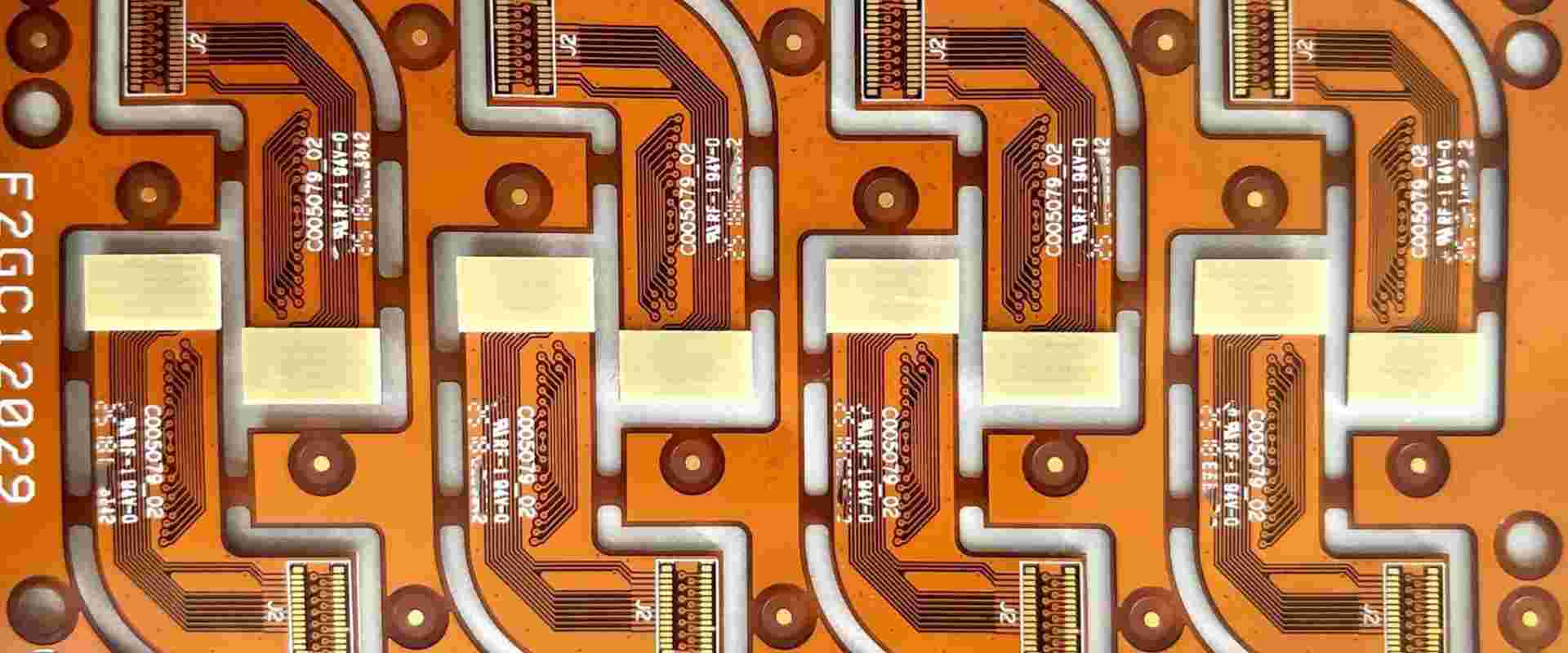
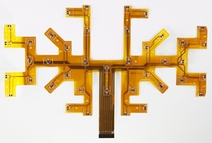
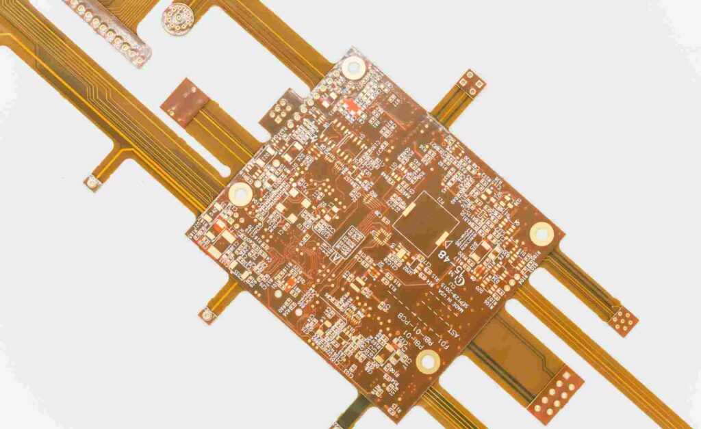
Flexible printed circuit boards (flex PCBs) play an important role in modern electronics by enabling connections between components in tight spaces. Flex PCBs utilize conductive traces on a flexible substrate that can bend and twist. Vias are plated through holes that allow signals to travel between layers of a multilayer flex PCB. Proper via design is crucial for ensuring reliability and performance. This article provides best practices and considerations when designing vias in flex PCBs.
Via Basics
Vias provide vertical interconnections between layers in a flex PCB. They are holes that are plated with copper to electrically connect the layers. The key aspects of via design include:
Via Location
Vias should be placed at intersections of traces requiring an interlayer connection. They should also be located close to component pads when traces need to change layers to reach the pad. This minimizes stub lengths.
Via Size
The drill diameter for a via hole should match the width of the traces it is connecting. Larger vias are preferable for handling high currents. Smaller vias save space but require thinner plating. Minimum size is usually 8-10 mils.
Pad Size
A larger annular ring pad around the via barrel strengthens the connection and allows more solder paste for reflow. But it also increases capacitance and takes up space. Typical pad diameters range from 14-25 mils larger than the drill diameter.
Plating Thickness
Vias require plated copper thicknesses of at least 1 oz (35 μm) but 3 oz (105 μm) or more is better for reliability. Thicker plating reduces resistance and handled higher currents.
Via Reliability Challenges
Vias in flex PCBs face stresses that can compromise reliability:
Thermal Cycling
Heating and cooling cycles create stresses due to CTE mismatch between materials. Flexing applies further stress. This can fracture solder joints and cause cracks or seperation.
Dynamic Flexing
Repeated bending and twisting of a flex PCB applies loads onto vias. This can cause copper fatigue and cracks leading to open circuits.
Vibration Forces
Vibration applies cyclic loads onto vias that can worsen cracks and lift off plating over time, increasing resistance.
Solder Reflow Issues
Poor solder fillet shapes, voids, or cracks in solder joints can occur due to solder beading on large pads. This reduces strength under dynamic loads.
Optimizing Specific Aspects of Via Design
Careful attention to detail in via design goes a long way towards enhancing flex PCB reliability:
Layer Transitions
- Stagger overlapping vias when changing layers to avoid tombstoning during reflow.
- Use teardrop shapes on pads to improve solder fillet shape and strength.
- Place ground or power vias adjacent to signal vias to act as faraday cages.
Solder Mask
- Use solder mask defined (SMD) pads so solder mask overlaps etched pads. Improves registration.
- Pull back solder mask on pads to avoid beading and help solder flow.
- Be sure mask material can withstand flexing and temperature cycles. Liquid photoimageable mask is often used.
Pad Shapes
- Use oval pads instead of circular for better solder bonding to trace ends.
- Consider teardrop pads for traces changing layers to improve fillets.
- Thermal relief cutouts on large copper pours help avoid beading and cracks.
Plating
- 3 oz copper minimum thickness with 6-12 oz for high reliability applications like medical devices.
- Be sure plating is continuous between inner layer pads and outer via barrels.
- Plate the layer 1 reference plane above vias for robustness under dynamic bending.
Materials
- Use adhesives like acrylic or epoxy that can flex repeatedly without cracking at vias.
- Rogers flex PCB materials like Pyralux AP offer excellent thermal and bend cycle reliability.
- Kapton polyimide films provide robust base materials for high reliability needs.
Testing
- Perform IST and HAST testing to verify via and solder joint reliability under temperature cycling.
- Use lateral flexing tests on coupons to determine robustness.
- Vibration testing ensures via barrels can handle cyclic stresses.
Design Guidelines for Reliable Flex PCB Vias
Here are some key guidelines to follow when designing vias in flexible PCBs:
- Use minimum 8 mil drill diameter and 1 oz copper plating. Increase for high power/current.
- Via pads should extend at least 14-25 mils beyond drill diameter.
- Stagger vias when shifting between layers. Include teardrops and adjacent ground vias.
- Pull back solder mask from pad edges to avoid solder beading and voids.
- Oval pads improve solder joint strength to traces. Use teardrops on layer shifts. -Maximize copper plating thickness, up to 6-12 oz for dynamic bending applications.
- Place reference plane above vias on layer 1 to add strength during flexing.
- Choose robust flexible base materials like Pyralux or Kapton.
- Perform thermal cycling, flexing, and vibration testing on coupons to verify reliability.
Following these guidelines helps ensure vias have the necessary strength to withstand the stresses of dynamic flexing, temperature extremes, and vibration in end product use conditions.
Comparison of Via Construction Options
There are a few different ways flex PCB vias can be constructed. The pros and cons of each approach are summarized below:
| Via Type | Description | Pros | Cons |
|---|---|---|---|
| Through-Hole | Drilled through entire board, plated | Simple process | Not repairable if damaged |
| Blind | Drilled partially through board | Allows more layer connections | Requires drilling from each side |
| Buried | Drilled and plated during layer pressing | Saves space | Difficult process control |
| Filled | Plated then filled with epoxy | More robust, no air gaps | Potential voiding in fill |
| Tented | Drilled then covered with soldermask | Protects from enviroment | Hard to inspect visually |
Through-hole vias are the most straightforward and common, providing a balance of simplicity and reliability. Blind and buried vias allow for more layer interconnections but require multiple drilling steps. Filled vias prevent air gaps but have potential for inner voids. Tented vias protect from oxidation but cannot be easily inspected.
Factors Affecting Flex PCB Via Reliability
There are several factors that can influence the reliability and robustness of vias in flex circuits. These should be taken into account in the design process:
- Copper Plating Thickness – Thicker plating increases current capacity and cracking resistance. At least 1 oz (35 μm) plating should be used with 3 oz (105 μm) or greater for dynamic or high-reliability flex applications.
- Solder Paste Volume – Too little solder paste can lead to poor fillet formation while excessive paste causes beading. A 1:1 paste:pad ratio is recommended.
- Solder Mask Overlap – Controlling solder mask clearance is key to avoiding solder beading while maintaining pad coverage. A 4-8 mil overlap is typical.
- Via Spacing – Closely spaced vias concentrate stresses. Wider spacing helps dissipate cyclic loads and prevents cracks propagating between vias.
- Reinforcement Material – Adhesives like acrylic or epoxy must withstand flexing stresses. Kapton or polyimide films make robust base layers.
- Plating Barrels – Seams or nodules in the plated copper barrel can initiate cracking under dynamic loads. Uniform plating is essential.
- Annular Ring Width – Wider pad rings around the via barrel provide more bonding area to strengthen the connection.
Careful attention to each of these factors improves the reliability and lifespan of vias in flex PCB designs.
Testing Flex PCB Via Reliability
To verify flex PCB via integrity under representative operating conditions, various tests can be performed:
- Thermal Cycling – Subjects boards to temperature extremes and thermal shocks that induce via stresses. Common tests are -55°C to 125°C over 1000 cycles.
- Highly Accelerated Stress Test (HAST) – Exposes boards to humidity, pressure, and temperature up to 130°C for accelerated life testing. Checks for electrochemical migration and solder joint integrity issues.
- Interconnect Stress Test (IST) – Applies -55°C to 125°C temperature cycling while simultaneously flexing boards dynamically. This accurately simulates stresses in real-world use.
- Vibration Testing – Shakes boards at various frequencies and accelerations to verify via and solder joint reliability under vibration loads.
- Flexure Testing – Bends coupons or full boards through arcs of 0.5-2 mm to ensure robustness under dynamic flexing conditions.
- Cross-Section Analysis – Cutting cross-sections of vias and inspecting under a microscope reveals plating quality, solder fill, and potential cracks.
Using these lab qualification tests allows via and solder joint defects to be caught during the design phase rather than after production and deployment to the field.
FQA
What minimum copper plating thickness should be used for flex PCB vias?
At least 1 oz (35 μm) plating should be used. For dynamic flexing or high reliability applications, 3 oz (105 μm) or thicker plating up to 6-12 oz is recommended.
How are blind and buried vias formed in multilayer flex PCBs?
Blind vias are drilled part way through from one side. Buried vias are drilled and plated during the layer lamination process before outer layers are bonded. This requires precise laser drilling when layers are still separate.
What are the main advantages of filled vias?
Filling vias with epoxy eliminates air gaps that can allow cracks to propagate. It also provides extra mechanical strength of the solder joint and barrel. But improper fill techniques can lead to interior voids.
Why is solder mask clearance important around vias?
Pulling back solder mask from the pad edge avoids solder beading which causes non-uniform filler and weak points. But solder mask overlap is still needed for registration and preventing oxidation. 4-8 mil clearance is typical.
What are common tests used to qualify flex PCB via reliability?
Thermal cycling, dynamic flexure cycling, vibration testing, and tests like HAST and IST are commonly used to simulate stresses seen in use conditions. Cross-section analysis also validates construction quality.
Conclusion
Vias enable routing between layers in multilayer flex PCBs but also introduce reliability risks from stresses like dynamic flexing and temperature cycling. Careful attention to via location, size, plating, solder mask design, pad shapes, and materials selection helps maximize robustness and product lifespan. Following best practice design guidelines combined with rigorous testing helps ensure flex circuits perform reliably over billions of use cycles. With the right construction, flexible PCBs can meet the rigorous demands of applications from consumer electronics to mission-critical aerospace systems.


Leave a Reply