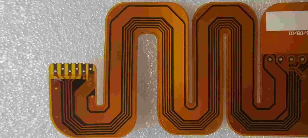
A flex PCB (flexible printed circuit board) is a type of PCB that is flexible and can bend or fold. It is made of very thin layers of copper traces on a flexible dielectric substrate. Flex PCBs allow for more compact and dynamic circuit design and are commonly used in consumer electronics, medical devices, aerospace applications etc.
One of the key elements of a flex PCB is the coverlay. The coverlay is a thin, flexible dielectric layer that covers and protects the traces on the flex PCB. In this article, we will take an in-depth look at flex PCB coverlay – what it is, its properties, materials, types, lamination process and more.
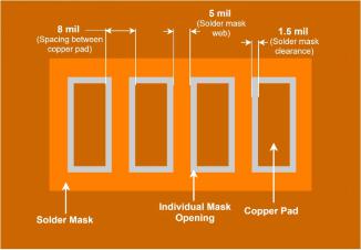
What is Flex PCB Coverlay?
A flex PCB coverlay, also known as a flex coverlay, is a protective layer that covers the conductive copper traces on the flex PCB. It serves multiple functions:
- Mechanical protection – It protects the thin and fragile copper traces from physical damage during handling and assembly.
- Electrical insulation – It provides electrical isolation between adjacent traces to prevent short circuits.
- Environmental protection – It seals and insulates the copper traces from environmental factors like moisture, chemicals etc.
In simpler terms, the coverlay covers up and insulates the intricate wiring patterns on the flex circuit, just like how insulation covers wire in cabling applications.<div align=”center”>
| Layer | Description |
|---|---|
| Copper Traces | Patterned copper forming conductive paths |
| Adhesive | To bond coverlay to base substrate |
| Coverlay | Thin flexible dielectric layer |
| Base Substrate | Flexible dielectric substrate (polyimide) |
Why is Coverlay Used in Flex PCBs?
Unlike rigid PCBs that have solder mask as a protective coating, flex PCBs use coverlay because of the following reasons:
- Thinner material – Coverlay films are thinner (around 12-25 μm) compared to typical solder mask (30-40 μm). This allows maintaining overall flexibility and thinness of the flex PCB.
- More flexible – Coverlay materials like polyimide are highly flexible to match the base substrate’s properties. This ensures bending doesn’t crack the protective coating.
- Lower processing temperature – Coverlay lamination needs lower temperature (around 190°C) versus solder mask curing (above 200°C) to avoid heat damage to the thin flex substrate.
- Easier visual inspection – Coverlay provides good contrast between traces and substrate for easier visual inspection of the flex PCB.
- Creep resistance – Polyimide coverlay has higher creep resistance than solder mask at elevated operating temperatures. This maintains long-term insulation performance.
Properties of Flex PCB Coverlay
The coverlay material used should exhibit the following properties for effective mechanical and electrical performance:
Flexibility
The coverlay should be flexible enough to bend, fold or flex along with the base polyimide substrate of the flex PCB without cracking or breaking. Typically, 2-3X more flexible than base material.
Electrical Properties
- High dielectric strength (>10 kV/mm) to prevent electrical breakdown at trace operation voltages
- High insulation resistance (>10^12 ohm-cm ) for effective electrical separation between adjacent traces
- Compatible dielectric constant (3-4) to maintain designed trace impedance
Thermal Properties
- High glass transition temperature (>150°C) for thermal stability in PCB assembly and operation at elevated temperatures
- Compatible CTE (coefficient of thermal expansion) to minimize thermal stress between trace and coverlay
Chemical Resistance
The coverlay must resist chemicals like solvents, acids, alkalis that the flex PCB may be exposed to during processing and operation.
Thin and Consistent Thickness
Typical coverlay thickness is around 12 to 25 μm. Thinner coverlay enables more compact and thinner flex PCB construction. The coverlay should also have a consistent, uniform thickness for reliable insulation.
Materials Used as Flex PCB Coverlay
Some common materials used as coverlay in flex PCBs are:
Polyimide
Polyimide film is the most commonly used coverlay material in flex PCBs. Some key properties:
- Excellent flexibility and bend radius
- High electrical insulation with dielectric strength of >300 V/mil
- High thermal stability with glass transition temperature >300°C
- Chemical and flame resistance
- Good soldering heat resistance
- Available in different thickness like 12.5 μm, 25 μm etc.
Popular brands of polyimide coverlay include DuPontTM Kapton®, Ube UPILEX®, Kaneka Apical® etc.
Acrylic
Acrylic coverlay provides a more economical option, though with lower thermal capability than polyimide. It has the following features:
- Moderate flexibility and bend radius
- Dielectric strength around 200 V/mil
- Glass transition temperature around 105°C – 125°C
- More limited chemical resistance versus polyimide
- Lower processing temperature saves energy
- Available in thickness down to 9 μm
Silicone
Silicone coverlay offers very high flexibility and low temperature lamination capability. Key properties:
- Excellent flexibility even down to 1 mm bend radius
- Moderate dielectric strength around 100V/mil
- Low glass transition temperature <90°C
- Poor chemical and heat resistance versus other coverlay
- Laminates at room temperature; no curing needed
Silicone coverlay allows small bend radius and 3D shaping of flex PCBs.
LCP (Liquid Crystal Polymer)
LCP films offer very high temperature capability as coverlay. Typical properties:
- High temperature resistance, with glass transition temperature ~300°C
- Low CTE provides excellent thermal-mechanical stability
- Very low moisture absorption compared to polyimide
- Expensive material option, mostly used in specialized flex PCBs
Coverlay Types
Flex PCB coverlay is available in different types depending on requirements:
Single Sided
Single sided coverlay has adhesive on one side of the film. It is applied on one side of the flex PCB to cover either the top or bottom of traces. Simple and economical option.
Double Sided
Double sided coverlay has adhesive on both sides. This allows lamination onto both sides of flex PCB to cover traces on top and bottom layers. Provides insulation on both sides.
Non-Adhesive
The coverlay film has no adhesive layer applied. Adhesive is screen printed separately onto the flex PCB before applying the coverlay. Provides more flexibility in coverlay application.
Supported
The coverlay film is temporarily bonded to a support layer like polyester during handling, and peeled off during lamination. Offers easier handling of thin coverlay films down to 12 μm thickness.
Non-Supported
The coverlay film is used standalone without any temporary bonded support layer. Suitable for thicker coverlay films above 18 μm.
Coverlay Lamination Process
The coverlay is precisely laminated over the flex PCB copper traces using the following steps:
- Surface Treatment – The flex PCB surface is chemically treated to enhance coverlay adhesion. Common treatments include sodium or plasma etching.
- Adhesive Application – For non-adhesive coverlay, screen printing is used to apply a thin layer of adhesive like acrylic or epoxy on the flex PCB surface.
- Coverlay Attachment – The coverlay film is precisely positioned over the flex PCB surface and nip rolled to attach it. Some temporary tacking can be used to hold the coverlay in place.
- Autoclave Pressing – The assembly is vacuum bagged and pressed in an autoclave to thoroughly bond the coverlay to the base substrate. Temperature of 180°C – 200°C and pressure around 300 – 500 psi is applied.
- Curing – For adhesive-based coverlays, elevated temperature curing for around 60 to 120 minutes is used to fully crosslink the adhesive and finalize bonding.
- Singulation – After lamination, individual flex PCB circuits are cut out from the panel using routing, laser cutting etc.
| Step | Description |
|---|---|
| 1 | Flex PCB Surface Treatment |
| 2 | Adhesive Application |
| 3 | Coverlay Attachment |
| 4 | Autoclave Pressing |
| 5 | Curing |
| 6 | Singulation |
This precise lamination process results in a tightly bonded coverlay protecting the copper traces, to enable a working flex PCB.
Coverlay Design Considerations
To optimize flex PCB performance, the following coverlay design practices should be followed:
- Minimize the number of coverlay layers and thickness to optimize flexibility.
- Allow adequate trace openings in coverlay for soldering pads, connectors etc.
- Coverlay cutouts also needed in flex-to-rigid PCB interfaces to prevent cracking.
- Use generous fillets and openings at flex fold areas to prevent coverlay or trace cracks.
- Index the coverlay properly to flex PCB layers to ensure accurate trace insulation.
- Account for coverlay shrinkage during lamination while designing.
- Keep coverlay bonded area to ~20% of panel area to enable easier lamination.
Proper coverlay design is essential to harness its protective benefits while minimizing impact on flex PCB flexibility or functionality.
Advantages and Disadvantages of Coverlay
Some key benefits and limitations of using coverlay in flex PCBs:
Advantages
- Provides excellent trace insulation and isolation
- Protects thin copper traces from physical damage
- Long-term reliability under mechanical flexing
- Withstands PCB assembly processes like soldering
- Enables visual inspection of trace defects
- Allows flexible circuit patterning on both sides
Disadvantages
- Adds thickness and stiffness versus uncovered traces
- Careful design needed around folds and bends
- Precise alignment and lamination process required
- Limited chemical and thermal resistance versus rigid PCB coatings
- Relatively expensive compared to solder mask
FQA
Here are some frequently asked questions about flex PCB coverlay:
Q: What is the typical thickness of coverlay used in flex PCBs?
A: Coverlay thickness typically ranges from 12 μm to 25 μm. Thinner 12-15 μm coverlay allows maximum flexibility while 25 μm provides better insulation and protection.
Q: Does coverlay delaminate or detach from the base substrate?
A: Properly laminated coverlay with suitable surface treatment should not delaminate during flexing. But factors like improper treatment, contamination, flex cracks etc. can cause localized delamination defects over time.
Q: What are some alternatives to polyimide coverlay?
A: Other common coverlay materials include acrylic, silicone and LCP films. Each has specific advantages in factors like cost, flexibility, thermal performance that make them viable for certain applications.
Q: What coverlay openings are required on the flex PCB?
A: Openings in the coverlay layer are required at points connecting to other components. This includes openings for solder pads, connectors, testpoints etc. to allow access to the traces.
Q: How many coverlay layers can be applied on a flex PCB?
A: For simplest construction, one coverlay layer on one side is typical. Two coverlay layers (one on each side) are possible for insulating both sides of traces. More layers are usually avoided due to impact on flexibility.
Conclusion
The coverlay is a critical component that enables reliable performance of flex PCBs in demanding applications. By protecting the copper traces and providing insulation between conductors, it allows flexible circuits to survive long-term bending and harsh environments. With a deeper understanding of coverlay materials, properties and design considerations, engineers can effectively utilize it while optimizing cost and reliability of flex PCB assemblies.


Leave a Reply