Introduction to Flex PCB Assembly
Flexible printed circuit boards (Flex PCBs) have gained significant popularity in recent years due to their versatility and ability to conform to various shapes and sizes. Flex PCB assembly has become an essential process for many industries, including consumer electronics, medical devices, automotive, and aerospace. In this comprehensive article, we will delve into the world of flex PCB assembly and provide you with valuable insights on how to achieve a wonderful PCB.
Understanding Flex PCBs
What are Flex PCBs?
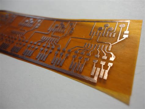
Flex PCBs are printed circuit boards that are designed to be flexible and bendable. Unlike traditional rigid PCBs, flex PCBs are made from thin, flexible materials such as polyimide or polyester. This flexibility allows them to be used in applications where space is limited, or where the PCB needs to conform to a specific shape.
Advantages of Flex PCBs
Flex PCBs offer several advantages over rigid PCBs, including:
- Improved reliability: Flex PCBs are less prone to cracking or breaking due to their flexibility, making them more reliable in harsh environments.
- Reduced weight and size: Flex PCBs are thinner and lighter than rigid PCBs, making them ideal for applications where weight and size are critical factors.
- Enhanced design flexibility: Flex PCBs can be bent, folded, or twisted to fit into tight spaces or conform to unique shapes, allowing for more creative and innovative designs.
- Increased signal integrity: Flex PCBs can reduce signal interference and improve signal integrity by allowing shorter, more direct signal paths.
Types of Flex PCBs
There are three main types of flex PCBs:
- Single-sided flex PCBs: These PCBs have conductive traces on only one side of the flexible substrate.
- Double-sided flex PCBs: These PCBs have conductive traces on both sides of the flexible substrate.
- Multi-layer flex PCBs: These PCBs consist of multiple layers of flexible substrates with conductive traces, allowing for more complex designs and higher component density.

Flex PCB Assembly Process
Design Considerations
Before beginning the flex PCB assembly process, it is crucial to consider several design factors:
- Material selection: Choose the appropriate flexible substrate material based on the application requirements, such as temperature range, flexibility, and durability.
- Trace width and spacing: Ensure that the trace width and spacing are optimized for the specific application to minimize signal interference and maintain signal integrity.
- Bend radius: Determine the minimum bend radius required for the flex PCB to avoid damaging the traces or components during the assembly process.
- Component placement: Carefully plan the component placement to minimize stress on the components and traces during flexing.
Fabrication Steps
The flex PCB assembly process involves several key steps:
- Substrate preparation: The flexible substrate is cleaned and treated to ensure proper adhesion of the conductive traces.
- Trace patterning: The conductive traces are created on the substrate using various methods, such as photolithography, screen printing, or etching.
- Via formation: Vias are created to interconnect the layers of a multi-layer flex PCB.
- Coverlay application: A protective coverlay is applied to the flex PCB to insulate and protect the conductive traces.
- Component placement: Surface mount and through-hole components are placed on the flex PCB using automated pick-and-place machines or manual soldering.
- Soldering: The components are soldered onto the flex PCB using reflow or wave soldering techniques.
- Cleaning and inspection: The assembled flex PCB is cleaned to remove any flux residue and inspected for defects or shorts.
Soldering Techniques
Soldering is a critical step in the flex PCB assembly process. There are two primary soldering techniques used:
- Reflow soldering: This method involves applying solder paste to the pads, placing the components, and then heating the entire assembly in a reflow oven to melt the solder and create a bond between the components and the pads.
- Wave soldering: This method is used for through-hole components and involves passing the flex PCB over a wave of molten solder, which creates a connection between the component leads and the PCB pads.
Quality Control and Testing
To ensure the quality and reliability of the assembled flex PCB, several quality control and testing procedures should be implemented:
- Visual inspection: A thorough visual inspection should be performed to identify any visible defects, such as poor soldering, misaligned components, or damaged traces.
- Automated optical inspection (AOI): AOI systems use high-resolution cameras and image processing algorithms to detect surface-level defects that may be missed during visual inspection.
- X-ray inspection: X-ray inspection is used to detect internal defects, such as voids or bridging, in solder joints or components.
- Electrical testing: Various electrical tests, such as continuity, insulation resistance, and functional testing, are performed to ensure that the flex PCB meets the specified electrical requirements.

Best Practices for Flex PCB Assembly
To achieve a wonderful flex PCB, follow these best practices:
- Work with experienced flex PCB manufacturers and assemblers who have a proven track record of producing high-quality flex PCBs.
- Provide clear and detailed design specifications to the manufacturer, including material requirements, trace width and spacing, bend radius, and component placement.
- Use appropriate soldering techniques and materials to ensure reliable and robust solder joints.
- Implement a comprehensive quality control and testing plan to catch any defects early in the assembly process.
- Consider the end-use environment and application requirements when designing and assembling the flex PCB to ensure optimal performance and reliability.

Common Challenges and Solutions
Flex PCB assembly can present several challenges, but with the right approach, these challenges can be overcome:
Challenge 1: Maintaining Bend Radius
Ensuring that the flex PCB maintains the required bend radius during assembly and use can be challenging.
Solution: Use reinforcement materials, such as stiffeners or adhesives, to support the flex PCB in areas where bending occurs. Also, consider designing the flex PCB with a larger bend radius than the minimum required to provide a safety margin.
Challenge 2: Preventing Component Cracking
Components mounted on flex PCBs are susceptible to cracking due to the stresses induced by bending.
Solution: Use flexible components whenever possible, and place components in areas of the flex PCB that experience minimal bending. Additionally, consider using underfill materials to provide additional support and stress relief for components.
Challenge 3: Handling and Processing
Flex PCBs can be more delicate than rigid PCBs, making handling and processing more challenging.
Solution: Use specialized handling equipment and techniques, such as vacuum or pneumatic grippers, to minimize the risk of damaging the flex PCB during assembly. Also, ensure that the assembly personnel are properly trained in handling flex PCBs.
Future Trends in Flex PCB Assembly
As technology continues to advance, several trends are shaping the future of flex PCB assembly:
- Increased adoption of 3D printing: 3D printing technologies, such as direct write and aerosol jet printing, are being explored for creating conductive traces on flexible substrates, enabling faster prototyping and more complex designs.
- Growing demand for wearable electronics: The rise of wearable devices is driving the demand for smaller, more flexible, and more reliable flex PCBs that can withstand the rigors of daily wear.
- Advances in materials science: New materials, such as stretchable conductors and self-healing polymers, are being developed to enhance the performance and durability of flex PCBs in challenging environments.
- Integration of sensors and antennas: Flex PCBs are increasingly being used to integrate sensors and antennas directly onto the PCB, enabling new applications in the Internet of Things (IoT) and wireless communication.
Frequently Asked Questions (FAQ)
-
Q: What is the typical turnaround time for flex PCB assembly?
A: The turnaround time for flex PCB assembly can vary depending on the complexity of the design, the materials used, and the manufacturer’s workload. Typical turnaround times range from 2-4 weeks, but expedited services may be available for urgent projects. -
Q: Can flex PCBs be reworked or repaired?
A: Yes, flex PCBs can be reworked or repaired, but the process can be more challenging than with rigid PCBs. Specialized tools and techniques, such as hot air rework stations and precision soldering irons, are often required to avoid damaging the delicate traces or components. -
Q: How do I select the right flex PCB manufacturer for my project?
A: When selecting a flex PCB manufacturer, consider factors such as their experience with flex PCBs, their manufacturing capabilities, their quality control processes, and their customer support. Look for manufacturers with a proven track record of producing high-quality flex PCBs and who are willing to work closely with you to ensure your project’s success. -
Q: What is the cost difference between flex PCBs and rigid PCBs?
A: Flex PCBs are generally more expensive than rigid PCBs due to the specialized materials, equipment, and processes required for their fabrication and assembly. However, the cost difference can vary depending on the specific design requirements and production volume. In some cases, the benefits of using flex PCBs, such as improved reliability and space savings, can outweigh the increased cost. -
Q: Can flex PCBs be used in harsh environments?
A: Yes, flex PCBs can be designed and assembled to withstand harsh environments, such as extreme temperatures, vibrations, and exposure to chemicals. The key is to select the appropriate materials, components, and assembly techniques that can withstand the specific environmental challenges. Working closely with an experienced flex PCB manufacturer can help ensure that your flex PCB is optimized for your application’s unique requirements.
Conclusion
Flex PCB assembly is a complex process that requires careful consideration of design, materials, and manufacturing techniques. By understanding the advantages and challenges of flex PCBs, and by following best practices and partnering with experienced manufacturers, you can achieve a wonderful PCB that meets your application’s unique requirements. As technology continues to advance, flex PCBs will play an increasingly important role in enabling new and innovative products across a wide range of industries.


Leave a Reply