Introduction to Flex Coverlays
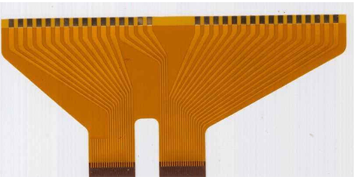
A flex coverlay, also known as a flexible coverlay, is a thin, flexible dielectric film that is laminated onto printed circuit boards (PCBs) to protect the conductive circuitry. Flex coverlays provide electrical insulation and protect against environmental contamination like moisture, dust, chemicals, and physical damage. They are commonly used in flexible PCBs as well as rigid-flex boards, which combine rigid and flexible PCB technology into one design.
Flex coverlays offer several benefits:
- Protection – Coverlays shield conductive traces from short circuits, environmental factors, and physical damage. This improves reliability and longevity.
- Insulation – Coverlays separate closely spaced conductors to prevent electrical shorts. This enables higher circuit densities.
- Flexibility – Thin coverlay materials (25-75μm) allow flexing without damage to circuits. This increases design freedom.
- Aesthetics – Coverlays can hide intricate circuitry for a cleaner, more visually appealing PCB.
With innovations in materials science, flex coverlays today have expanded capabilities to meet modern design requirements. Let’s look at common types of flex coverlays used in PCBs.
Types of Flex Coverlays
There are several categories of flex coverlay materials to consider:
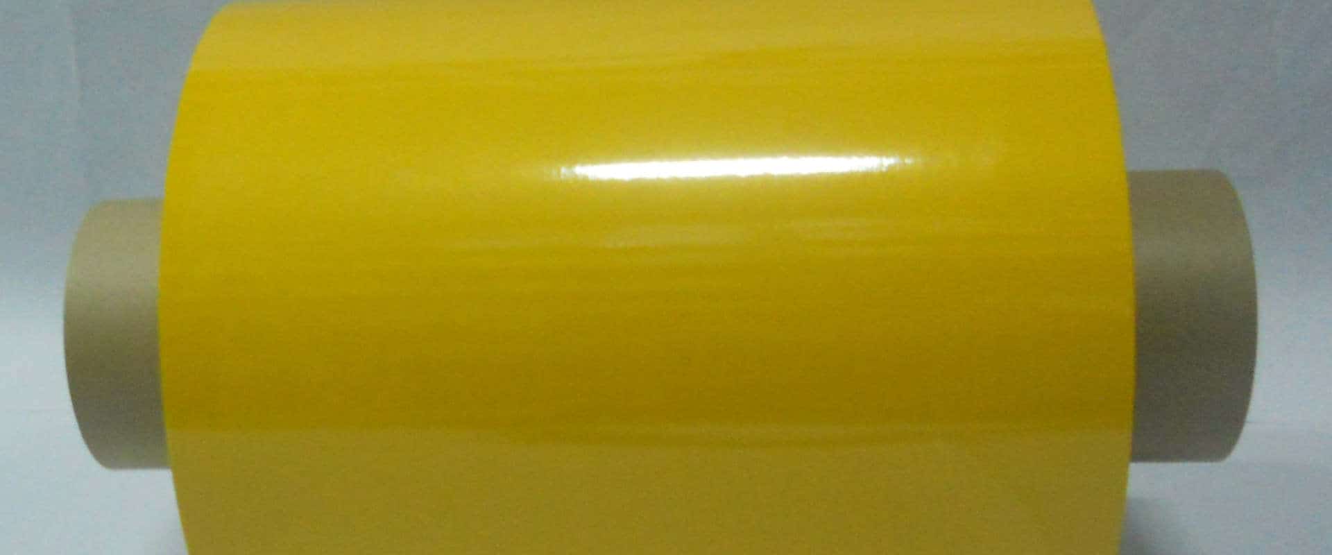
Polyimide
Polyimide film is the most common coverlay material. Offered under brands like DuPontTM Kapton®, polyimide provides:
- Exceptional chemical resistance
- High dielectric strength
- Excellent thermal stability
- Wide operating temperature range (-269°C to 400°C)
Polyimide has high tensile strength to accommodate repeated flexing. It has good dimensional stability over a wide temperature range. Polyimide coverlays are available in various thicknesses from 12μm to over 75μm.
Polyester
Polyester (PET) coverlays offer:
- Low moisture absorption
- Good dielectric properties
- Economic alternative to polyimide
Polyester coverlays have operating temperatures up to 150°C and are typically 25-50μm thick. Brands like Melinex® are common.
Liquid Photoimageable
Liquid photoimageable (LPI) coverlays provide patterned openings for solder mask, bonding windows, and flex/rigid transitions. Benefits include:
- Eliminates secondary lamination steps
- Improves registration accuracy
- Allows smaller openings versus mechanical methods
- Wide range of polymer options (acrylic, urethane, epoxy, silicone)
LPI coverlays are coated on the PCB surface, imaged, and cured. Dry film and electrophoretic photopolymers are also options.
UV Curable
UV curable coverlays utilize acrylated epoxy, urethane, and silicone formulations. Advantages are:
- Single exposure for fast processing
- No VOCs
- Thickness 25-125μm
They cure rapidly under UV light without excessive heating. UV coverlays work well for multilayer flex, rigid-flex, and advanced HDI boards.
Conductive
Conductive coverlays have metal particles or graphite dispersed in the polymer. They are used when shielding or ground planes are needed on the outer surfaces. Common polymers used are acrylic and epoxy.
Bondply
Bondply coverlays have thermoplastic adhesive on one side to bond directly to the PCB surface. This eliminates the need for separate adhesive lamination steps. Bondply materials include polyimide, polyester, and liquid photoimageable polymers.
Coverlay Properties
Several key properties should be considered when selecting a flex coverlay:
Dielectric Strength
This refers to the material’s electrical insulating capability. Dielectric strength is expressed in volts/mil (V/mil) and indicates the voltage needed to electrically break down the material. Most coverlay films have dielectric strengths from 4000-10,000 V/mil.
Dielectric Constant
The dielectric constant (Dk) indicates how easily the coverlay material transmits electric flux. Lower Dk allows closer conductor spacing for higher densities. Polyimide has a low Dk of 3.4-3.6 at 1 MHz.
Dissipation Factor
Also called loss tangent, dissipation factor (Df) indicates how much electromagnetic energy is absorbed in the coverlay. Lower Df values are better for high frequency applications. Polyimide’s typical Df is 0.002-0.005.
Thermal Properties
Important thermal properties include maximum operating temperature, coefficient of thermal expansion (CTE), and thermal conductivity. These determine how the material physically responds to temperature changes. Polyimide withstands over 400°C continuously.
Mechanical Properties
Key mechanical characteristics are tensile strength, elongation, and flexural endurance. These indicate the coverlay’s durability under physical and bending stresses. Polyimide shows outstanding flex life, exceeding 100,000 cycles in testing.
Chemical Resistance
The coverlay material must resist corrosive or reactive chemicals it may contact during processing or use. Polyimide has broad chemical resistance and won’t stress crack.
Flammability Rating
Safety standards regulate flammability. Typically, UL 94 V-0 is required for consumer products. Polyimide films offer excellent flame resistance.
Environmental
“Green” factors like waste handling, recyclability, and eco-friendly production processes are growing considerations. Most coverlay suppliers now support environmental policies.
Coverlay Design Factors
Proper design is critical to utilize flex coverlays effectively. Here are key guidelines:
- Coverlay thickness should match board thickness to avoid surface irregularities. Select thinner coverlays (25-50μm) for maximum flexibility.
- Allow sufficient margin between conductors and coverlay edges for alignment tolerance and material movement during lamination. A minimum 2:1 ratio is recommended.
- Adhesion must withstand thermal and bending stresses. Ensure compatible adhesive and sufficient cure during lamination.
- Avoid rigid sections in dynamic flex areas. Use strategically placed flexible hinges.
- Isolate components from flexing zones to reduce stresses. Provide stress relief cutouts.
- Index pin holes accurately locate coverlays and boards. Allow +/- 0.4mm tolerance for alignment.
- Surface finishes must be compatible. Most coverlays bond to electrodeposited or rolled copper.
- Design test coupons on panel peripheries to verify coverlay properties like adhesion, thickness, and dielectric strength.
Thoroughly testing prototypes is critical before advancing to production. Environmental stress screening (ESS) evaluates durability under temperature cycling, vibration, and bending stresses.
Coverlay Processing Considerations
Fabricating boards with flex coverlays requires specialized processing:
Surface Preparation
The PCB surface must be free of moisture, oils, oxides, and particulates to enable adhesive bonding. Typical steps include cleaning, plasma etch, and chemical surface treatments.
Lamination
Lamination adheres the coverlay to the PCB using heat and pressure. Lamination presses use polished, heated platens to gradually cure adhesive while removing air entrapment and wrinkles. Vacuum assist is common.
Registration
Accurate alignment between coverlay and conductors is critical to prevent shorts. Registration holes or fiducials on the PCB and coverlay film enable precise positioning. Vision systems further improve accuracy.
Imaging
For photoimageable coverlays, UV light imaging transfers the desired pattern. Laser direct imaging (LDI) offers high resolution and reliability. Phototools and masks are traditionally used.
Developing
Unexposed polymer is dissolved to create open areas in the coverlay for solder mask openings, bonding windows, etc. Spray developers are typically used.
Etching
Etching removes polymer residue from patterned openings in the coverlay to ensure clean exposures of the underlying PCB conductors. Microetching is required.
Curing
Curing crosslinks and sets the polymer chains to finalize patterning. Thermal curing in ovens is most common. Some coverlays use UV or other energy curing methods.
Testing
Electrical testing and microscopy inspection verifies coverlay quality. Parameters like dielectric strength, insulation resistance, thickness uniformity, and defect detection are evaluated.
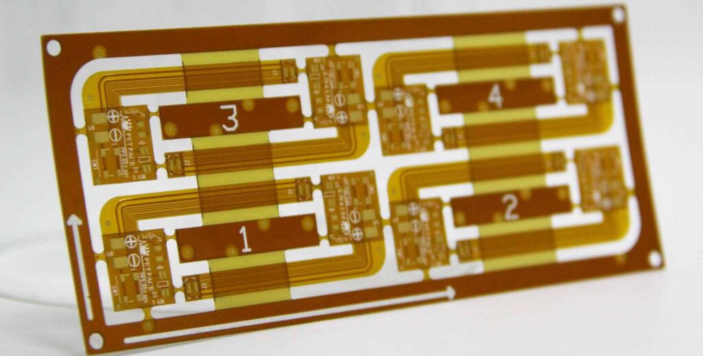
The Role of Coverlays in Rigid-Flex PCBs
Coverlays take on increased importance with rigid-flex PCBs. These boards have both rigid sections for components and connectors, combined with dynamic flexing zones to enable three-dimensional configurations and flexing component interfaces.
Polyimide coverlays are ideal for rigid-flex designs. Flexible yet robust, polyimide withstands repeated bending stresses. It bonds reliably to dissimilar materials at the rigid-flex interfaces. Polyimide’s wide temperature range tolerates lead-free soldering and other processing extremes.
In rigid-flex boards, coverlays serve key functions:
Insulation – Coverlays insulate conductors at layer transitions between rigid and flex zones where dielectrics change. This prevents shorts between adjacent conductors.
Wear Resistance – Thin polyimide coverlays protect conductors from abrasion during dynamic flexing motion. They prevent conductor damage that could cause opens and intermittent contacts.
Stiffening – Coverlays build up section thickness to create more rigid zones on board peripheries. They counteract bending stresses and prevent conductor fractures.
Marking – Coverlays provide a surface for component legends, fiducials, board outline, and other printed markings to guide assembly. Marks withstand handling and exposure that can damage conductors.
Packaging – Coverlays seal conductors from environmental contamination during shipment and assembly. They help prevent oxidation and solderability issues.
Aesthetics – Coverlays hide complex circuitry patterns underneath for a smooth, controlled appearance. This allows flexing motion without visible deformation of conductors.
Proper coverlay integration is imperative in rigid-flex designs:
- Dynamic sections should utilize thin (12-25μm) polyimide coverlay for maximum flex life and bend radius.
- Rigid sections can support thicker coverlay up to 75μm as needed for insulation and stiffness.
- Coverlay thickness must transition gradually between sections to prevent surface irregularities and stresses.
- Sufficient adhesive margins are required at board and coverlay edges.
- Motion cycles must be within rated flexural endurance limits.
With the right coverlay strategy, rigid-flex PCBs can maximize design innovation. The protective insulation and flexibility of coverlays enable compact form factors with reliable dynamic bends and flexing component integration.
Coverlay Issues to Avoid
Though highly reliable when applied properly, coverlays can also create problems if not designed and integrated with care:
Wrinkling – Wrinkles can occur from inadequate adhesive, trapped gases during lamination, or material instability under temperature changes. Rework may be needed.
Delamination – Lack of adhesive or poor bonding promotes separation of coverlay and conductors. Flexing accelerates delamination.
Crazing – Network of fine cracks in coverlay surface from stresses beyond material limits. Caused by heat shock, flexing, or impact. Can propagate to conductors underneath.
Tenting – Coverlay sagging into plated through holes can make hole walls concave. Impedes plating throwing power and reduces reliability.
Stains – Water marks, adhesive residue, fingerprints, and other stains can affect aesthetics and ability to print or mark the coverlay surface.
Outgassing – Release of absorbed moisture and gases during lamination or thermal excursions causes surface defects like bubbles and pinholes.
Curling – Imbalanced stresses make coverlay curl up at edges and corners, exposing conductors. Thermal mismatches are a common cause.
Scorching – Excessive heat during soldering can selectively burn (scorch) coverlay and damage properties.
Summary
As PCBs become denser with demanding design requirements, high-performance coverlay materials are more important than ever to ensure reliability and functionality. Coverlays protect, insulate, and enable innovative circuit constructs ranging from multilayer boards to advanced rigid-flex configurations. Matching coverlay properties and design integration strategies to the application is the key to success. With sound engineering practice, coverlays will continue meeting emerging needs well into the future.
Frequently Asked Questions
Q: What are some key advantages of using a coverlay?
A: The main benefits of using a coverlay are protecting the PCB’s conductors, providing electrical insulation between conductors, enabling flexibility and dynamic motion in flex PCBs, and giving a smooth, controlled aesthetic appearance.
Q: How thick are typical coverlay materials used in PCB fabrication?
A: Coverlays range from 12μm to over 75μm in thickness. Thinner coverlays of 25-50μm are preferred for flexible PCBs to maximize bend radius. Thicker coverlays are used where more insulation or stiffness is required.
Q: What are some leading types of coverlay materials available?
A: Major coverlay types include polyimide films like Kapton, polyester films such as Melinex, liquid photoimageable coverlays, UV curable polymers, conductive coverlays, and bondply coverlays with adhesive already applied.
Q: What are some ways coverlays fail that engineers should design to avoid?
A: Common coverlay failures are wrinkling, delamination from the PCB surface, crazing cracks from stresses, curling up at edges, tenting into plated holes, and scorching from excess heat during soldering.
Q: Why are coverlays especially critical for rigid-flex PCB designs?
A: For rigid-flex PCBs, coverlays insulate layer transitions between rigid and flex areas, prevent conductor damage from repeated flexing, stiffen board sections, and enable dynamic motion capabilities. Polyimide is ideal for rigid-flex coverlays.


Leave a Reply