Introduction to Flat Flex PCBs
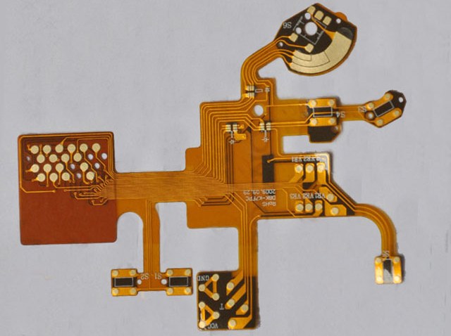
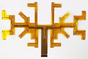
A flat flex PCB (also known as FFC or flexible flat cable) is a type of flexible printed circuit board made of thin and flexible dielectric materials. Flat flex PCBs can be bent, twisted, folded or flexed to fit into tight spaces and 3D packages where rigid PCBs would be unfeasible.
Compared to rigid PCBs, the thin and flexible construction of flat flex PCBs make them ideal for applications where space is very limited but interconnectivity is required. Their flexibility also makes them useful for moving components like printers and industrial equipment.
Key Features of Flat Flex PCBs
- Thin and lightweight – Flat flex PCBs have a thickness typically between 50-100 microns. This allows them to fit into the tightest spaces.
- Highly flexible – Can be bent, folded and twisted repeatedly to route around obstacles. Flex life > 50,000 cycles.
- Reliable connections – Copper traces are laminated so they don’t crack when flexed. Ensure reliable connectivity.
- Simple connectivity – Integrated into complex devices as jumpers and connectors for electronics like cameras, disk drives etc.
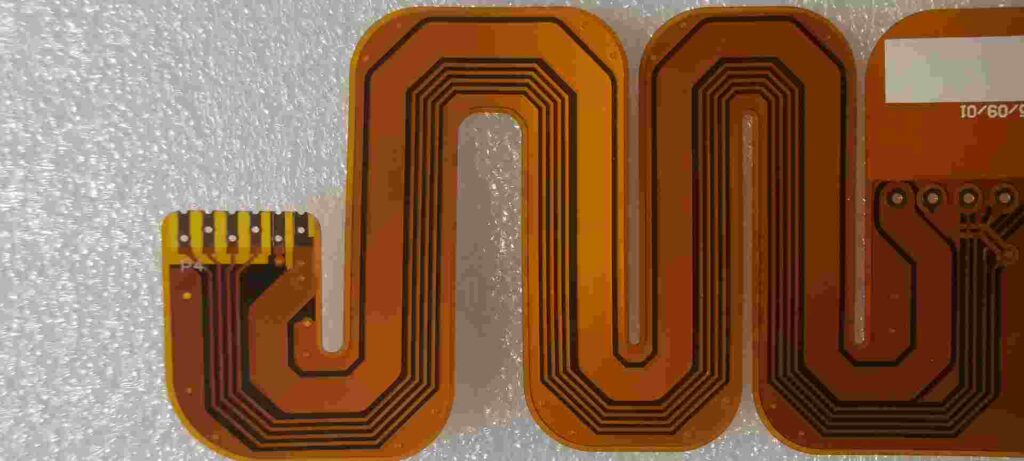
- Customizable – Can be fabricated in different shapes like zig-zag or meandered to specification.
Construction and Composition
Flat flex PCB construction consists of flexible conductive and dielectric materials laminated together:
- Base Material – Flexible plastic substrates like polyimide, PEN, PET etc. Provide mechanical support.
- Conductors – Copper foil rolled annealed soft for flexibility. Other options like aluminum or silver plating.
- Cover layer – Additional insulator bonded on top for protection. Liquid photoimageable or dry film.
- Stiffener – Optional thicker plastic or metal layer to provide rigidity in parts.
Typical Flat Flex PCB Stackup
| Layer | Description | Thickness |
|---|---|---|
| Cover Coat | Liquid photoimageable or dry film for insulation/protection | 12-25 microns |
| Copper Foil | Rolled annealed copper, can be plated for durability | 12-35 microns |
| Base Material | Flexible plastic like polyimide, PET, PEN etc | 25-100 microns |
| Adhesive | Bond inner layers together | 25-50 microns |
| Stiffener | Optional plastic or metal for rigidity in sections | 50-300 microns |
Total thickness – As low as 50 microns, up to 600 microns depending on layer and stackup requirements.
Flat Flex PCB Design Rules
To achieve a reliable, manufacturable flat flex PCB layout, designers need to follow specific design for manufacturing (DFM) rules:
Trace Width/Spacing
Narrow trace/space is possible due to thinner copper foils. Minimum trace width and spacing down to 100 micron lines/spaces.
Bending Radius
Avoid 90 degree or sharp bends. Minimum bending radius is typically > 10X dielectric thickness. Gradual curves are preferred.
Copper Coverage
Avoid large copper areas (>200mm2) which affect flex life. Copper grids or meshes are an alternative.
Stiffener Placement
Stiffeners can be used in selected regions for support. Avoid sharp corners or ends.
adhesive Voids
Adhesive voids under copper traces can cause flex cracks. Specify no voids under conductors.
Following these guidelines optimizes flat flex PCB reliability under dynamic flexing conditions.
Flat Flex PCB Applications
With their small footprint and excellent flexibility, flat flex PCBs are widely used in:
- Consumer electronics – Cameras, printers, hard drives, display screens etc. Interconnections for electronics and mechanical linkages.
- Industrial – Robotics, automation equipment. Flexible connectivity for moving parts.
- Medical – Hearing aids, wearables, implants. Can fit into tiniest spaces.
- Automotive – Sensors, gauges, battery management systems. Withstand vibration/shock environments.
- Aerospace – Avionics, guidance systems, space applications. Rugged yet light weight.
Flat Flex PCB Manufacturing Process
Flat flex PCB fabrication follows a lithographic process similar to rigid PCBs but using flexible materials able to withstand flexing:
Step 1 – Lamination
The base dielectric material and copper foils are precisely laminated together under heat and pressure.
Step 2 – Photolithography
A photosensitive dry film or liquid photoresist is applied on the copper layers and then exposed to UV light through a mask.
Step 3 – Etching
The unexposed photoresist is developed away, exposing the underlying copper for etching into the desired circuit pattern.
Step 4 – Strip and Clean
The remaining photoresist is stripped away and the PCB is clean of processing residues.
Step 5 – Cover Layer
An insulating cover layer like LPI solder mask is applied over the exposed traces/pads for insulation and marking.
Step 6 – Finishing
Final finishes like HAL, immersion gold or ENIG can be applied to exposed pads/lands for solderability or contact.
This subtractive process allows the custom etching of copper circuitry to manufacture flat flex PCBs.
Factors to Consider in Flat Flex PCB Design
Here are some important considerations when designing flat flex PCBs:
- Intended application and operating environment. This defines the required flex life, temperature range etc.
- Number of flexible layers needed – Single sided, double sided or multilayer. Drives complexity.
- Integrating rigid sections if needed for connectors, boards etc. Requires managing rigid-flex boundary.
- Minimum bend radius and dynamic flex requirements. Ensures reliable mechanical performance.
- Matching thermal expansion coefficients between flexible and rigid parts. Reduces stresses.
- Electrical requirements like high speed signals, controlled impedances, shielding etc.
- Protecting tracks in high wear areas. Such as coverlayers, vias, stiffeners etc.
- EMI containment strategies like ground planes and shielding solutions.
Paying attention to these parameters when designing optimizes the flat flex PCB for its application and environment.
Flat Flex PCB Cost Drivers
The costs of producing flexible printed circuits depend on:
- Design complexity – More layers or smaller features require more process steps. Dense multi-layer circuits are more expensive.
- Materials – Base material thickness, type and thickness of copper foils. Flexible materials cost more than rigid.
- Quantity – Small batch prototyping has high NRE costs. Larger production volumes drive down unit price.
- Finishes and coatings – Special platings like gold or advanced coverlay add cost.
- Testing – Rigorous inspection and testing (like X-ray, AOI) adds cost but reduces defects.
- Tolerances – Tighter tolerances require more process controls and increase costs.
- Lead times – Rush orders or quick turnaround times increase manufacturing costs.
Working closely with your PCB supplier to optimize these parameters can help reduce flat flex PCB costs for a project.
FQA
What are some key advantages of flat flex PCBs?
Some key advantages of flat flex PCBs:
- Extremely thin – As low as 50 microns thickness – for tight spaces
- Highly flexible – Can be folded and bent over 10,000 times – dynamic movement
- Reliable connections – Laminated copper does not crack under flexing
- Customizable – Fabricated in different shapes like zig-zag or meandered
- Simple integration – Used as jumpers or complex interconnects for electronics
How are flat flex PCBs different from rigid PCBs?
Flat flex PCBs differ from rigid PCBs in the following ways:
- Use thin flexible dielectric substrate materials like polyimide instead of rigid FR4
- Employ rolled annealed copper foils that are thinner and more ductile
- Fabrication allows dynamic flexing without cracking conductive traces
- Significantly thinner with tight spacing – 50 micron lines/spaces
- Can be bent and twisted to route through 3D spaces
- Withstand vibration, shock, and frequent flexing conditions
- Used where rigidity limits PCB design – ex. in movable components
What are some good design practices for flat flex PCBs?
Some good design practices for flat flex PCBs:
- Avoid 90 degree bends – use minimum bend radius >10X dielectric thickness
- Limit large copper planes which reduce flex life – use grids/meshes instead
- Manage number of layers – more layers increases complexity and cost
- Incorporate stiffeners/rigid sections only where needed
- Ensure no adhesive voids under traces – causes flex cracking failure
- Analyze thermal expansion differences between flex and rigid sections
- Protect high wear areas like vias and tracks with coverlayers
- Incorporate stress relief features into designs with dynamic flexing
What are the typical steps in manufacturing flat flex PCBs?
Typical manufacturing steps for flat flex PCBs:
- Lamination – Bonding of dielectric base material and copper foils
- Lithography – Applying photoresist and patterning circuits using UV light
- Etching – Chemically etching away unwanted copper
- Stripping – Removing all photoresist residues
- Cover layer – Laminating insulating coverlay over traces
- Finishing – Applying platings/coatings for soldering or contact
- Testing – Rigorous inspection of traces, dimensions and defects
- Singulation – Carefully cutting into individual PCBs
What are some typical applications of flat flex PCBs?
Typical applications of flat flex PCBs:
- Consumer electronics – cameras, printers, hard drives
- Industrial – robotics, machinery, automation equipment
- Medical – implants, hearing aids, wearables
- Transportation – sensors and electronics in auto, marine, aerospace
- Instrumentation – interconnect various electronics
- Defense – guidance, radar and communication systems
The thin, flexible construction makes flat flex PCBs suitable for integrating electronics in tight spaces with reliability.


Leave a Reply