Introduction to FastPrintPCB
FastPrintPCB is a revolutionary technology that has transformed the way printed circuit boards (PCBs) are manufactured. It enables the rapid production of high-quality PCBs, significantly reducing lead times and costs. In this article, we will explore the key factors that contribute to creating the perfect FastPrintPCB and how you can optimize your PCB design and manufacturing process.
Understanding the FastPrintPCB Process
How FastPrintPCB Works
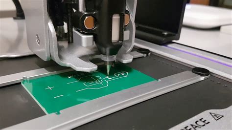
FastPrintPCB utilizes advanced manufacturing techniques to streamline the PCB production process. The process involves the following steps:
- PCB Design: The PCB layout is designed using specialized software, ensuring optimal component placement and routing.
- Printing: The PCB design is printed onto a substrate material using high-precision inkjet or screen printing technology.
- Curing: The printed PCB undergoes a curing process to solidify the conductive traces and ensure proper adhesion to the substrate.
- Etching: Any excess conductive material is removed through an etching process, leaving only the desired circuit pattern.
- Finishing: The PCB undergoes additional finishing processes, such as solder mask application and surface finish, to enhance its durability and functionality.
Benefits of FastPrintPCB
FastPrintPCB offers several advantages over traditional PCB manufacturing methods:
- Rapid Prototyping: FastPrintPCB enables quick prototyping, allowing designers to test and iterate their designs in a shorter timeframe.
- Cost-Effective: The streamlined process reduces material waste and eliminates the need for expensive tooling, resulting in lower production costs.
- Flexibility: FastPrintPCB supports a wide range of substrate materials and can accommodate complex designs with fine features and high component density.
- Environmental Friendliness: The process minimizes the use of harsh chemicals and reduces waste, making it an eco-friendly choice for PCB manufacturing.

Factors Affecting FastPrintPCB Quality
To achieve the perfect FastPrintPCB, several factors must be considered and optimized. Let’s explore these factors in detail.
PCB Design Considerations
Component Placement
Proper component placement is crucial for optimal PCB performance. When designing your PCB, consider the following:
- Group components based on their functionality to minimize the length of interconnections.
- Place components in a way that facilitates efficient routing and reduces signal interference.
- Ensure adequate spacing between components to allow for proper soldering and heat dissipation.
Trace Width and Spacing
The width and spacing of the conductive traces on your PCB play a significant role in signal integrity and manufacturability. Keep in mind:
- Use appropriate trace widths based on the current carrying requirements of your circuit.
- Maintain sufficient spacing between traces to prevent short circuits and signal crosstalk.
- Adhere to the minimum trace width and spacing guidelines specified by your FastPrintPCB manufacturer.
Via Placement and Size
Vias are used to connect traces between different layers of a multi-layer PCB. When placing vias, consider:
- Minimize the number of vias to reduce manufacturing complexity and improve signal integrity.
- Use appropriate via sizes based on the current carrying requirements and the capabilities of your FastPrintPCB manufacturer.
- Place vias strategically to minimize their impact on signal routing and component placement.
Material Selection
Substrate Material
The choice of substrate material is critical for the performance and reliability of your FastPrintPCB. Common substrate materials include:
| Material | Characteristics | Applications |
|---|---|---|
| FR-4 | Low cost, good mechanical strength, suitable for general-purpose PCBs | Consumer electronics, industrial control systems |
| Polyimide | High temperature resistance, flexibility, suitable for flexible PCBs | Aerospace, military, wearable devices |
| Aluminum | Excellent thermal conductivity, used for heat dissipation | Power electronics, LED lighting |
Consider the electrical, mechanical, and thermal requirements of your application when selecting the appropriate substrate material.
Conductive Ink
The conductive ink used in FastPrintPCB plays a vital role in the conductivity and durability of the printed traces. Key considerations include:
- Ink Composition: Choose a conductive ink that offers high conductivity, good adhesion to the substrate, and compatibility with the printing process.
- Curing Requirements: Ensure that the selected ink can be properly cured using the available equipment and within the desired timeframe.
- Environmental Stability: Consider the environmental conditions your PCB will be exposed to and select an ink that can withstand those conditions.
Printing Process Optimization
Printer Settings
Optimizing the printer settings is essential for achieving high-quality FastPrintPCB. Consider the following:
- Resolution: Use the highest possible resolution that your printer supports to achieve fine features and precise trace dimensions.
- Layer Thickness: Adjust the layer thickness based on the requirements of your PCB design and the capabilities of your printer.
- Printing Speed: Find the optimal balance between printing speed and quality. Faster printing may result in lower resolution and potential defects.
Curing Conditions
Proper curing of the printed conductive traces is crucial for their conductivity and adhesion to the substrate. Key factors include:
- Temperature: Ensure that the curing temperature is within the recommended range for the selected ink and substrate material.
- Duration: Allow sufficient time for the ink to fully cure and achieve optimal conductivity.
- Atmosphere: Some inks may require specific atmospheric conditions, such as inert gas or vacuum, for proper curing.

Quality Control and Testing
To ensure the reliability and functionality of your FastPrintPCB, implementing proper quality control measures and thorough testing is essential.
Visual Inspection
Perform a visual inspection of the printed PCB to identify any obvious defects, such as:
- Incomplete or inconsistent traces
- Short circuits or open connections
- Misaligned or missing components
Electrical Testing
Conduct electrical tests to verify the functionality and performance of your FastPrintPCB. Common tests include:
- Continuity Test: Verify that all desired connections are intact and there are no unintended short circuits.
- Resistance Test: Measure the resistance of traces to ensure they meet the specified requirements.
- Insulation Resistance Test: Check the insulation resistance between adjacent traces and layers to prevent leakage currents.
Functional Testing
Perform functional testing to validate that your FastPrintPCB operates as intended in its target application. This may involve:
- Powering up the PCB and verifying the expected behavior of connected components.
- Running test scripts or automated test equipment to exercise various functions of the PCB.
- Subjecting the PCB to environmental stress tests, such as temperature cycling or vibration, to assess its reliability.

Frequently Asked Questions (FAQ)
-
Q: What is the minimum feature size achievable with FastPrintPCB?
A: The minimum feature size depends on the capabilities of the specific FastPrintPCB manufacturer and the selected printing technology. Typically, feature sizes as small as 50-100 microns can be achieved with high-end FastPrintPCB systems. -
Q: Can FastPrintPCB be used for multi-layer PCBs?
A: Yes, FastPrintPCB technology can be used to manufacture multi-layer PCBs. The process involves printing and curing each layer separately and then laminating them together to form the final multi-layer structure. -
Q: How does the cost of FastPrintPCB compare to traditional PCB manufacturing methods?
A: FastPrintPCB is generally more cost-effective than traditional PCB manufacturing methods, especially for low-volume production and prototyping. The reduced setup costs, faster turnaround times, and lower material waste contribute to the overall cost savings. -
Q: What are the limitations of FastPrintPCB technology?
A: FastPrintPCB may have limitations in terms of the maximum PCB size, the thickness of the substrate material, and the ability to incorporate certain advanced features such as buried or blind vias. It is important to consult with your FastPrintPCB manufacturer to understand their specific capabilities and limitations. -
Q: How long does it take to manufacture a PCB using FastPrintPCB?
A: The manufacturing time for FastPrintPCB is significantly shorter compared to traditional PCB manufacturing methods. Depending on the complexity of the design and the capabilities of the manufacturer, a FastPrintPCB can be produced in a matter of hours to a few days.
Conclusion
FastPrintPCB technology has revolutionized the way PCBs are manufactured, offering rapid prototyping, cost-effectiveness, and flexibility. To achieve the perfect FastPrintPCB, careful consideration must be given to PCB design, material selection, printing process optimization, and quality control measures.
By understanding the key factors that influence FastPrintPCB quality and following best practices in design and manufacturing, you can unlock the full potential of this innovative technology. Whether you are a hobbyist, a startup, or an established electronics company, FastPrintPCB provides a powerful tool to bring your ideas to life quickly and efficiently.
As FastPrintPCB continues to evolve and mature, we can expect to see even more advanced capabilities and applications in the future. Embracing this technology and staying up-to-date with the latest developments will position you at the forefront of the rapidly evolving world of PCB manufacturing.


Leave a Reply