What is a PCB Layout?
A Printed Circuit Board (PCB) layout is a detailed design of the physical arrangement of electronic components and their interconnections on a PCB. It is a crucial step in the PCB manufacturing process, as it determines the functionality, reliability, and manufacturability of the final product. The PCB layout process involves translating the schematic diagram of the circuit into a physical representation that can be fabricated.
Key Elements of a PCB Layout
- Component Placement
- Routing
- Copper Pour
- Silkscreen
- Solder Mask
Why is PCB Layout Design Important?
A well-designed PCB layout ensures that the circuit functions as intended, minimizes electromagnetic interference (EMI), and maximizes the reliability and longevity of the product. Poor PCB layout design can lead to various issues, such as:
- Signal integrity problems
- Electromagnetic compatibility (EMC) issues
- Thermal management challenges
- Manufacturing difficulties
- Increased production costs

PCB Layout Design Process
1. Gathering Requirements
Before starting the PCB layout design, it is essential to gather all the necessary information and requirements, such as:
- Schematic diagram
- Bill of Materials (BOM)
- PCB size and shape constraints
- Layer stack-up
- Manufacturing capabilities and limitations
2. Component Placement
The first step in PCB layout design is to place the components on the board. The placement should consider factors such as:
- Functional grouping of components
- Signal flow
- Thermal management
- Mechanical constraints
- Manufacturing considerations
Best Practices for Component Placement
| Practice | Description |
|---|---|
| Functional Grouping | Place components that work together in close proximity to minimize signal path length and reduce noise. |
| Signal Flow | Arrange components to follow the logical signal flow, from input to output, to minimize signal crossing and improve signal integrity. |
| Thermal Management | Place heat-generating components away from temperature-sensitive components and provide adequate thermal relief. |
| Mechanical Constraints | Consider the mechanical constraints, such as connector locations, mounting holes, and component heights, when placing components. |
| Manufacturing Considerations | Ensure that the component placement allows for efficient assembly and soldering processes, and provides sufficient clearance for testing and rework. |
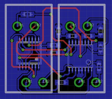
3. Routing
After component placement, the next step is to route the interconnections between the components. Routing involves creating copper traces on the PCB layers to establish electrical connections according to the schematic diagram. The main objectives of routing are to:
- Minimize signal path length
- Reduce crosstalk and EMI
- Ensure signal integrity
- Optimize manufacturability
Routing Techniques
-
Manual Routing: The designer manually creates the traces using PCB layout software tools, providing full control over the trace geometry and placement.
-
Auto-Routing: PCB layout software tools can automatically route the traces based on predefined rules and constraints, saving time and effort. However, auto-routing may not always produce optimal results and may require manual refinement.
Routing Considerations
| Consideration | Description |
|---|---|
| Trace Width | Select appropriate trace widths based on the current carrying capacity and signal integrity requirements. |
| Trace Spacing | Maintain sufficient spacing between traces to minimize crosstalk and ensure manufacturability. |
| Via Placement | Minimize the number of vias and place them strategically to reduce signal degradation and improve manufacturability. |
| Layer Assignment | Assign signals to appropriate layers based on their characteristics and requirements, such as power, ground, and high-speed signals. |
| Length Matching | Match the lengths of critical signal traces to maintain signal integrity and timing. |
4. Copper Pour
Copper pour, also known as ground plane or power plane, is the process of filling unused areas of the PCB with copper. Copper pour serves several purposes:
- Provides a low-impedance return path for signals
- Reduces EMI and crosstalk
- Improves thermal dissipation
- Enhances mechanical stability
5. Silkscreen
Silkscreen is a layer of text and graphics printed on the PCB surface to provide information such as component designators, polarity markers, and assembly instructions. The silkscreen layer helps in the assembly and troubleshooting of the PCB.
6. Solder Mask
Solder mask is a protective layer applied over the copper traces and pads, leaving only the areas intended for soldering exposed. Solder mask serves the following purposes:
- Prevents solder bridges and short circuits
- Protects the copper from oxidation and corrosion
- Provides electrical insulation between adjacent traces
- Improves the PCB’s appearance

PCB Layer Stack-up
The PCB layer stack-up refers to the arrangement of copper layers and insulating materials that make up the PCB. The choice of layer stack-up depends on factors such as:
- Circuit complexity
- Signal integrity requirements
- EMC considerations
- Manufacturing capabilities
- Cost constraints
Common Layer Stack-up Configurations
| Layers | Description |
|---|---|
| Single-layer | A single copper layer on one side of the substrate, suitable for simple circuits. |
| Double-layer | Two copper layers, one on each side of the substrate, with through-hole components. |
| Four-layer | Two inner copper layers sandwiched between two outer layers, providing better signal integrity and EMI performance. |
| Six-layer and above | Multiple copper layers with alternating signal and power/ground planes, used for complex high-speed designs. |

Design for Manufacturing (DFM)
Design for Manufacturing (DFM) is the practice of designing PCBs with consideration for the manufacturing process, aiming to minimize production issues and costs. Some key DFM guidelines include:
- Adhering to the manufacturer’s design rules and constraints
- Using standard component sizes and footprints
- Providing adequate spacing between components and traces
- Minimizing the number of unique components and footprints
- Using techniques such as panelization and fiducial markers to improve manufacturing efficiency
PCB Layout Software Tools
There are several PCB layout software tools available in the market, ranging from free and open-source to commercial and enterprise-level solutions. Some popular PCB layout software tools include:
- Altium Designer
- Cadence Allegro
- Mentor Graphics PADS
- KiCad (free and open-source)
- Eagle (free version available)
Frequently Asked Questions (FAQ)
1. What is the difference between a schematic and a PCB layout?
A schematic is a graphical representation of the electrical connections and components in a circuit, while a PCB layout is the physical arrangement of those components and connections on a printed circuit board.
2. Can I use auto-routing for my entire PCB layout?
While auto-routing can save time and effort, it may not always produce optimal results, especially for complex or high-speed designs. It is recommended to use a combination of manual and auto-routing, and to thoroughly review and refine the auto-routed traces.
3. How do I choose the appropriate trace width for my PCB layout?
The choice of trace width depends on factors such as the current carrying capacity, signal integrity requirements, and manufacturability. You can use online trace width calculators or consult with your PCB manufacturer to determine the appropriate trace widths for your design.
4. What is the purpose of a ground plane in a PCB layout?
A ground plane is a large area of copper that covers most of the PCB surface, usually on a dedicated layer. It provides a low-impedance return path for signals, reduces EMI and crosstalk, improves thermal dissipation, and enhances the mechanical stability of the PCB.
5. How can I ensure my PCB layout is manufacturable?
To ensure your PCB layout is manufacturable, follow the manufacturer’s design rules and constraints, use standard component sizes and footprints, provide adequate spacing between components and traces, minimize the number of unique components and footprints, and use techniques such as panelization and fiducial markers to improve manufacturing efficiency. It is also recommended to communicate with your PCB manufacturer throughout the design process to address any potential issues early on.


Leave a Reply