Introduction
A printed circuit board (PCB) serves as the foundation for electronics that require the mounting and interconnection of components. Flexible PCBs provide the ability to bend and flex the board during use, opening up possibilities for flexible and wearable electronics. Double sided flex PCBs take this a step further by allowing components and circuitry to be mounted on both sides of the thin flexible substrate.
In this article, we will explore what double sided flex PCBs are, their design and manufacturing considerations, and examine some of their uses and applications.
What are Double Sided Flex PCBs?
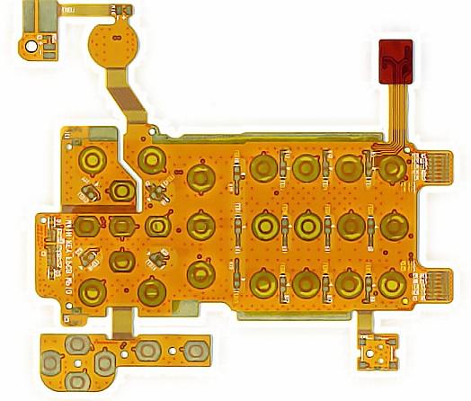
A double sided flex PCB is a type of flexible printed circuit board that allows components and circuit traces to be placed on both sides of the board. Here are some key properties of double sided flex PCBs:
- Flexible substrate material such as polyimide allows the board to bend and flex without damage.
- Circuits and components can be assembled on both top and bottom sides.
- Vias and plated through holes connect traces between the two sides.
- Typical thickness is around 0.05mm to 0.15mm.
- Can be bent or folded to fit the target application.
The flexible nature and small size makes double sided flex PCBs suitable for applications where a rigid board would be impractical. Wearable devices, medical devices, robotics, and consumer electronics can benefit from a thin, bendable circuit board that can accommodate components on both sides.
Design Considerations
Designing double sided flex PCBs requires special considerations, especially related to the flexible nature of the board:
Flexibility
The flexing of the board needs to be accounted for in the layout. Bending should occur only in designated bend areas, with components placed in rigid zones. Stiffeners may be used to control flexing in certain areas.
Layer Stackup
A typical stackup involves an inner copper layer with a polyimide dielectric layer on either side. Additional layers can be added for more complex designs.
Component Placement
Components need to be placed only in rigid areas of the board, avoiding any bend zones. It helps to place smaller components on the flexing areas.
Routing Traces
Traces should be routed in only one direction in flexing areas. Vias should have annular rings to protect against cracking.
Strain Relief
Providing strain relief in flexing regions prevents damage over repeated bending. This can be done with various geometric patterns in the copper layers.
Testing and Simulation
Prototyping and simulation helps verify the design performance under bending and flexing. Finite element analysis tools can predict stress and failure points.
Manufacturing Process
Double sided flex PCB fabrication involves specialized processes and steps:
Substrate Material
Polyimide is most commonly used due to its flexible properties and high heat resistance. Adhesives bond the polyimide layers.
Imaging and Etching
Photolithographic processes transfer the traces pattern onto the copper clad substrate. Etching then removes unwanted copper.
Registration
Precise alignment between layers is required to achieve interconnectivity between both sides. Lasers drill microvias.
Layer Alignment
Special care must be taken when aligning layers to ensure pads/traces match accurately between sides.
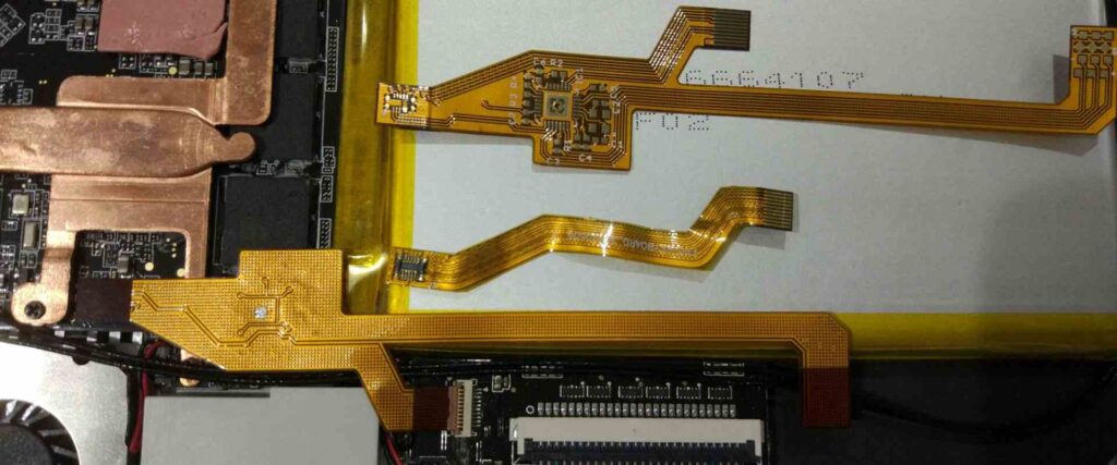
Component Assembly
SMT components are typically used. Reflow soldering attaches components. Care must be taken in handling the thin flexing boards.
Testing and Inspection
Electrical testing and optical inspection ensures boards are fabricated per the design specifications without any defects.
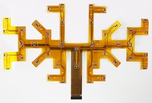
Applications and Uses
Some examples of how double sided flex PCBs are being used:
Wearable Devices
The compact, thin, and flexible nature makes them suitable for wearables such as fitness trackers and smart watches. Batteries and sensors can be integrated on both sides.
| Component | Placement |
|---|---|
| CPU | Rigid area |
| Sensors | Flexible area |
| Battery | Other side |
Medical Devices
For devices like hearing aids and glucose monitors, a thin, flexible circuit board can be comfortably worn on the body. Double sided flex allows more components in a smaller form factor.
Robotics
The ability to bend and flex opens up possibilities for robotic appendages and features. Sensors and actuators can be integrated onto the limbs.
| Component | Qty |
|---|---|
| Servo Motors | 4 |
| Force Sensors | 6 |
| Microcontroller | 1 |
Consumer Electronics
Double sided flex PCBs allow creative industrial design for mobile phones, laptops, and other consumer electronics that require flexible PCBs to fit in folding or unconventionally shaped devices.
Pros and Cons of Double Sided Flex PCBs
| Pros | Cons |
|---|---|
| Compact size and thin profile | More complex design and manufacturing |
| Flexibility allows creative form factors | Requires advanced CAD tools |
| High component density with double sided assembly | Limited flex life cycle |
| Allows for integrated rigid and flexible regions | Relatively higher cost |
| Ideal for wearable and flexible applications | Special handling required |
Conclusion
With their ability to incorporate circuits and components on both sides of a thin, flexible substrate, double sided flex PCBs open up opportunities for miniaturized and creative product designs. However, the flexible aspect introduces complexities in layout, simulation, and manufacturing that requires special expertise. As technology in flex PCBs matures, we can expect wider adoption in wearable devices, medical equipment, robotics, and consumer electronics where conventional rigid boards are not suitable.
Frequently Asked Questions
What are some key differences between rigid PCBs and flex PCBs?
Rigid PCBs use substrates like FR-4 that do not flex while flex PCBs use polyimide or other materials that allow for repeated bending. Rigid PCBs provide more structure while flex PCBs can fit into dynamic contours and spaces.
How are components mounted on double sided flex PCBs?
SMT components are commonly used with reflow soldering. Components are only placed in rigid areas, avoiding any bend zones. Smaller components can sometimes be carefully placed in flexing areas.
Are there limitations on the number of layers in double sided flex PCBs?
While 2 to 6 layers are typical, some complex designs use up to 12 layers. However, as layer counts increase, the board becomes thicker and less flexible. High layer counts also increase costs.
What are some best practices for routing traces in flexible PCBs?
Use curved traces instead of angles in flexing areas. Avoid vias in bend zones. Planes should be crosshatched for flexibility. Provide strain relief patterns along traces.
How are double sided flex PCBs tested?
They are electrically tested just like rigid PCBs. Additionally, samples are flexed repeatedly to validate bending performance. Finite element analysis simulation is also used.


Leave a Reply