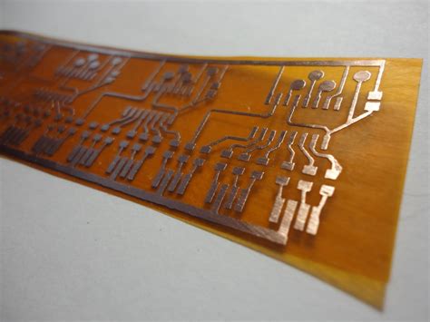
What is a Flexible PCB?
A flexible printed circuit board, also known as a Flex-PCB or FPC, is a type of PCB that uses a flexible plastic substrate instead of the rigid fiberglass material used in standard PCBs. This allows the circuit board to bend and flex without breaking, making it ideal for applications where the PCB needs to fit into a tight space, wrap around a curve, or withstand repeated flexing.
Flex-PCBs are commonly used in a wide range of products, including:
- Smartphones and tablets
- Wearable devices
- Medical devices
- Automotive electronics
- Aerospace and military equipment
Advantages of Flexible PCBs
Compared to traditional rigid PCBs, Flex-PCBs offer several key advantages:
-
Improved reliability: Flex-PCBs are more resistant to vibration and shock, which can help improve the overall reliability of the device.
-
Reduced weight and thickness: Because Flex-PCBs use a thinner substrate material, they can be much lighter and thinner than rigid PCBs, which is important for applications where size and weight are critical factors.
-
Increased flexibility: Flex-PCBs can bend and flex without breaking, allowing them to fit into tight spaces or wrap around curves.
-
Better heat dissipation: Flex-PCBs can help improve heat dissipation by allowing heat to be spread out over a larger surface area.
-
Reduced assembly time: Flex-PCBs can often be assembled more quickly than rigid PCBs, since they can be folded or shaped to fit into the device enclosure.

Types of Flexible PCBs
There are several different types of Flex-PCBs, each with its own unique characteristics and applications:
| Type | Description | Applications |
|---|---|---|
| Single-sided Flex | A single layer of conductive traces on one side of the flexible substrate. | Simple low-cost applications, such as keyboards and remote controls. |
| Double-sided Flex | Conductive traces on both sides of the substrate, with plated through-holes connecting the two layers. | More complex applications that require higher density and functionality, such as camera modules and displays. |
| Multi-layer Flex | Three or more layers of conductive traces, separated by insulating layers and connected with plated through-holes. | High-density applications that require a large number of interconnects, such as smartphone motherboards and medical devices. |
| Rigid-Flex | A combination of rigid and flexible sections, with the flexible sections used to connect the rigid sections. | Applications that require both the stability of a rigid board and the flexibility of a Flex-PCB, such as aerospace and military equipment. |

Designing a Flexible PCB
Designing a Flex-PCB involves several key considerations that are different from designing a rigid PCB:
Material Selection
The first step in designing a Flex-PCB is to select the appropriate materials for the substrate, conductors, and cover layers. The most common substrate materials for Flex-PCBs are polyimide (PI) and polyester (PET), which offer a good balance of flexibility, durability, and cost.
For the conductive traces, copper is the most commonly used material, although other metals such as silver and gold can be used for specialized applications. The thickness of the copper layer will depend on the current-carrying requirements of the circuit, with thicker layers used for higher-current applications.
The cover layers, which protect the conductive traces and provide insulation, are typically made from a flexible solder mask material or a thin layer of polyimide.
Trace Width and Spacing
When designing the conductive traces for a Flex-PCB, it’s important to consider the minimum trace width and spacing that can be reliably manufactured. In general, Flex-PCBs can support trace widths and spacing down to about 3-4 mils (0.003-0.004 inches), although this will depend on the specific manufacturing process and the capabilities of the PCB fabricator.
It’s also important to consider the current-carrying requirements of the traces, as well as the potential for signal integrity issues such as crosstalk and impedance mismatch. In general, wider traces will have lower resistance and higher current-carrying capacity, but will also take up more space on the board.
Bend Radius
One of the key design considerations for Flex-PCBs is the minimum bend radius, which is the tightest radius that the board can be bent without damaging the conductive traces or the substrate material. The minimum bend radius will depend on the thickness and material properties of the substrate and the copper traces, as well as the number of layers in the board.
As a general rule of thumb, the minimum bend radius for a single-layer Flex-PCB should be at least 6 times the thickness of the board, while for a multi-layer board it should be at least 10 times the thickness. However, it’s always best to consult with the PCB fabricator to determine the specific bend radius requirements for your design.
Stiffeners and Strain Relief
In order to prevent damage to the Flex-PCB during bending and flexing, it’s often necessary to add stiffeners and strain relief features to the design. Stiffeners are typically made from a rigid material such as FR-4 or polyimide, and are used to reinforce the areas of the board that will be subject to the most stress during bending.
Strain relief features, such as curves or S-shapes in the traces, can also help to distribute the stress more evenly across the board and prevent damage to the traces.

Fabricating a Flexible PCB
Once you have completed the design of your Flex-PCB, the next step is to have it manufactured by a PCB fabricator. The fabrication process for Flex-PCBs is similar to that for rigid PCBs, but with a few key differences:
-
Substrate preparation: The flexible substrate material is cut to size and cleaned to remove any contaminants.
-
Copper lamination: A thin layer of copper is laminated onto the substrate using heat and pressure.
-
Patterning: The desired circuit pattern is transferred onto the copper layer using a photoresist and etching process.
-
Drilling: Any necessary holes are drilled through the board for component placement or interconnects.
-
Plating: The holes are plated with copper to create electrical connections between layers.
-
Solder mask application: A flexible solder mask is applied to the board to protect the copper traces and prevent short circuits.
-
Silkscreen printing: Any necessary text or graphics are printed onto the board using a silkscreen process.
-
Cutting and finishing: The completed board is cut to its final shape and any necessary finishing processes, such as surface plating or edge beveling, are performed.
Assembling a Flexible PCB
Once you have received your completed Flex-PCB from the fabricator, the next step is to assemble the components onto the board. The assembly process for Flex-PCBs is similar to that for rigid PCBs, but there are a few key considerations to keep in mind:
-
Component placement: When placing components onto a Flex-PCB, it’s important to consider the potential for stress on the components during bending and flexing. Components should be placed in areas of the board that will be subject to minimal stress, and should be oriented in a way that minimizes the risk of damage.
-
Soldering: Soldering components onto a Flex-PCB requires a gentle touch and a fine-tipped soldering iron. It’s important to use a low-temperature solder and to avoid applying too much heat, which can damage the flexible substrate.
-
Strain relief: To help prevent damage to the components and traces during flexing, it’s often necessary to add strain relief features to the assembly, such as adhesive or mechanical supports.
Testing and Troubleshooting
After assembling your Flex-PCB, it’s important to thoroughly test it to ensure that it is functioning properly. Some common testing methods for Flex-PCBs include:
-
Continuity testing: Using a multimeter to check for continuity between various points on the board to ensure that there are no open circuits or short circuits.
-
Functional testing: Powering up the board and testing its functionality to ensure that it is performing as expected.
-
Flexing testing: Bending and flexing the board to ensure that it can withstand the expected level of mechanical stress without damage.
If any issues are detected during testing, it may be necessary to troubleshoot the board to identify and fix the problem. Some common troubleshooting techniques for Flex-PCBs include:
-
Visual inspection: Carefully inspecting the board for any visible defects or damage, such as cracked traces or lifted pads.
-
Continuity testing: Using a multimeter to identify any open or short circuits that may be causing problems.
-
Component replacement: If a component is found to be faulty, it may need to be removed and replaced with a new one.
FAQs
-
What is the minimum bend radius for a Flex-PCB?
The minimum bend radius for a Flex-PCB depends on the thickness and material properties of the substrate and copper traces, as well as the number of layers in the board. As a general rule of thumb, the minimum bend radius for a single-layer Flex-PCB should be at least 6 times the thickness of the board, while for a multi-layer board it should be at least 10 times the thickness. However, it’s always best to consult with the PCB fabricator to determine the specific bend radius requirements for your design. -
Can I use regular solder on a Flex-PCB?
It’s generally not recommended to use regular solder on a Flex-PCB, as the high temperature required for melting the solder can damage the flexible substrate. Instead, it’s best to use a low-temperature solder specifically designed for use with Flex-PCBs. -
How do I prevent damage to my Flex-PCB during bending and flexing?
To help prevent damage to your Flex-PCB during bending and flexing, it’s important to design the board with strain relief features such as curves or S-shapes in the traces, and to add stiffeners and supports to the assembly where necessary. It’s also important to handle the board gently during assembly and use, and to avoid bending it beyond its maximum bend radius. -
Can I use the same design software for Flex-PCBs as I do for rigid PCBs?
Most PCB design software packages have specific tools and features for designing Flex-PCBs, such as the ability to define bend lines and specify the minimum bend radius. However, the overall design process is similar to that for rigid PCBs, so if you are already familiar with PCB design software, you should be able to easily adapt to designing Flex-PCBs. -
How do I choose the right Flex-PCB manufacturer?
When choosing a Flex-PCB manufacturer, it’s important to consider factors such as their experience with Flex-PCBs, their manufacturing capabilities and quality control processes, and their pricing and turnaround time. It’s also a good idea to request samples or references from previous customers to get a sense of the quality of their work. Finally, it’s important to communicate clearly with the manufacturer about your specific requirements and expectations for the project.
In conclusion, designing and fabricating a Flex-PCB can be a complex process, but with careful planning and attention to detail, it’s possible to create a high-quality, reliable flexible circuit board that meets your specific needs. By understanding the key design considerations, choosing the right materials and manufacturing processes, and following best practices for assembly and testing, you can ensure the success of your Flex-PCB project.


Leave a Reply