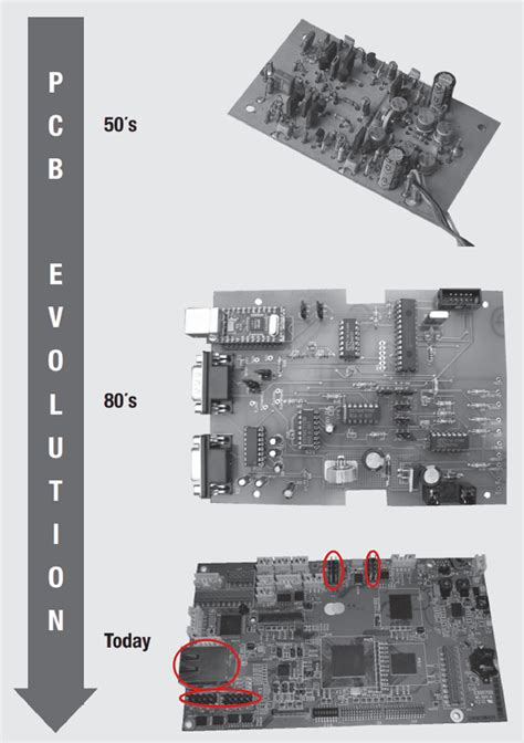
Introduction to PCB Evolution
Printed Circuit Boards (PCBs) have come a long way since their inception in the early 20th century. The evolution of PCBs has been driven by advancements in technology, changes in consumer demands, and the need for more efficient and reliable electronic devices. In this article, we will explore the development history and trends of PCBs, from their humble beginnings to the cutting-edge designs of today.
The Early Days of PCB Technology
The Invention of PCBs
The concept of PCBs can be traced back to the early 1900s when German inventor Albert Hanson filed a patent for a “printed wire” board in 1903. However, it wasn’t until the 1920s that Charles Ducas, an American inventor, created the first “printed circuit” by electroplating conductors onto an insulated substrate.
The Rise of Through-Hole Technology
In the 1940s, during World War II, the demand for more compact and reliable electronic devices led to the development of through-hole technology. This method involved drilling holes into the PCB and inserting components with wire leads, which were then soldered onto the board. Through-hole technology revolutionized the electronics industry and remained the standard for several decades.

The Evolution of PCB Manufacturing Processes
The Introduction of Surface Mount Technology (SMT)
In the 1960s, surface mount technology (SMT) emerged as an alternative to through-hole technology. SMT allowed components to be mounted directly onto the surface of the PCB, eliminating the need for drilled holes. This advancement led to smaller, more densely packed boards and faster assembly processes.
Advancements in PCB Materials
As PCB technology evolved, so did the materials used in their construction. Early PCBs were made from phenolic paper, but this was soon replaced by more durable materials like fiberglass and epoxy resin. In the 1970s, the introduction of flame-retardant materials improved the safety and reliability of PCBs.

The Rise of Multilayer PCBs
The Need for Increased Complexity
As electronic devices became more sophisticated, the need for more complex PCB designs grew. Multilayer PCBs, which consist of multiple layers of conductive and insulating materials, allowed for higher component density and improved signal integrity.
The Development of High-Density Interconnect (HDI) PCBs
In the 1990s, high-density interconnect (HDI) PCBs emerged as a solution to the increasing demands for smaller, more powerful electronic devices. HDI PCBs feature finer lines and spaces, smaller vias, and higher layer counts, enabling the creation of highly compact and complex designs.

Modern PCB Trends and Innovations
Flexible and Rigid-Flex PCBs
Flexible and rigid-flex PCBs have gained popularity in recent years due to their ability to conform to unique shapes and withstand repeated flexing. These PCBs are particularly useful in wearable electronics, medical devices, and aerospace applications.
The Internet of Things (IoT) and PCB Design
The rise of the Internet of Things (IoT) has had a significant impact on PCB design. IoT devices require small, low-power, and wireless-enabled PCBs, driving the development of new technologies like printed electronics and embedded components.
Sustainable and Eco-Friendly PCB Solutions
As environmental concerns grow, there has been a push for more sustainable and eco-friendly PCB solutions. This includes the use of recyclable materials, the reduction of hazardous substances, and the adoption of green manufacturing processes.
The Future of PCB Technology
Advancements in 3D Printing for PCBs
3D printing technology has the potential to revolutionize PCB manufacturing. By enabling the creation of complex, three-dimensional structures, 3D printing could lead to new PCB designs and faster prototyping processes.
The Integration of Artificial Intelligence (AI) in PCB Design
Artificial intelligence (AI) is poised to play a significant role in the future of PCB design. AI-powered tools could assist in optimizing PCB layouts, identifying potential design flaws, and streamlining the design process, ultimately leading to more efficient and reliable PCBs.
Frequently Asked Questions (FAQ)
-
Q: What are the main differences between through-hole and surface mount technology?
A: Through-hole technology involves inserting component leads through drilled holes in the PCB and soldering them on the opposite side. Surface mount technology (SMT) mounts components directly onto the surface of the PCB, allowing for smaller and more densely packed designs. -
Q: What are the advantages of multilayer PCBs?
A: Multilayer PCBs offer several advantages, including higher component density, improved signal integrity, and better electromagnetic interference (EMI) shielding. They also enable more complex designs and can reduce the overall size of electronic devices. -
Q: How have IoT devices influenced PCB design?
A: IoT devices have driven the demand for smaller, low-power, and wireless-enabled PCBs. This has led to the development of new technologies, such as printed electronics and embedded components, which enable the creation of compact and efficient PCBs for IoT applications. -
Q: What role does AI play in the future of PCB design?
A: AI-powered tools have the potential to streamline the PCB design process by assisting in layout optimization, identifying potential design flaws, and suggesting improvements. This could lead to more efficient and reliable PCBs, as well as faster time-to-market for electronic devices. -
Q: Why is there a growing interest in sustainable and eco-friendly PCB solutions?
A: As environmental concerns continue to grow, there is an increasing demand for sustainable and eco-friendly PCB solutions. This includes the use of recyclable materials, the reduction of hazardous substances, and the adoption of green manufacturing processes to minimize the environmental impact of PCB production.
Conclusion
The evolution of PCBs has been a remarkable journey, driven by technological advancements, changing consumer demands, and the need for more efficient and reliable electronic devices. From the early days of through-hole technology to the cutting-edge designs of today, PCBs have continually adapted to meet the needs of an ever-evolving industry.
As we look to the future, trends like flexible and rigid-flex PCBs, IoT-driven designs, and sustainable solutions will continue to shape the development of PCBs. Moreover, emerging technologies like 3D printing and AI have the potential to revolutionize the way we design and manufacture PCBs, leading to new possibilities and innovations in the field.
In conclusion, the development history and trends of PCBs showcase the remarkable progress and adaptability of this essential technology. As electronic devices continue to evolve, so too will PCBs, ensuring that they remain at the heart of our increasingly connected and technology-driven world.


Leave a Reply