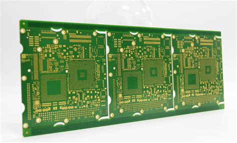
Introduction to PCBs and Their Types
Printed Circuit Boards (PCBs) are essential components in modern electronics, providing a reliable and efficient way to connect electronic components. PCBs come in various types, each designed to cater to specific requirements and applications. Two notable types are standard PCBs and Thick Copper PCBs.
What is a Standard PCB?
A standard PCB is the most common type of printed circuit board used in electronic devices. These boards typically feature copper traces with a thickness ranging from 1 oz to 2 oz per square foot (305 to 610 micrometers). Standard PCBs are suitable for a wide range of applications, including consumer electronics, telecommunications, and industrial control systems.
What is a Thick Copper PCB?
Thick copper PCBs, also known as Heavy Copper PCBs, are printed circuit boards with copper traces thicker than those found in standard PCBs. The copper thickness in thick copper PCBs can range from 3 oz to 20 oz per square foot (915 to 6100 micrometers). These boards are designed to handle high currents, provide better heat dissipation, and offer improved mechanical stability.
Differences Between Standard PCB and Thick Copper PCB
While both standard and thick copper PCBs serve the purpose of connecting electronic components, they have distinct differences that make them suitable for different applications. Let’s explore these differences in detail.
Copper Thickness
The primary difference between standard and thick copper PCBs lies in the thickness of the copper traces.
| PCB Type | Copper Thickness Range |
|---|---|
| Standard PCB | 1 oz to 2 oz per square foot (305 to 610 micrometers) |
| Thick Copper PCB | 3 oz to 20 oz per square foot (915 to 6100 micrometers) |
The increased copper thickness in thick copper PCBs provides several advantages, such as:
- Higher current-carrying capacity
- Better heat dissipation
- Improved mechanical stability
- Reduced resistance and voltage drop
Current Carrying Capacity
One of the main reasons for using thick copper PCBs is their ability to handle higher currents compared to standard PCBs. The thicker copper traces allow for increased current flow without overheating or causing damage to the board.
| PCB Type | Current Carrying Capacity |
|---|---|
| Standard PCB | Limited to low to moderate currents |
| Thick Copper PCB | Can handle high currents, suitable for power electronics |
Thermal Management
Thick copper PCBs offer superior thermal management capabilities compared to standard PCBs. The increased copper thickness allows for better heat dissipation, preventing components from overheating and prolonging the lifespan of the electronic device.
| PCB Type | Thermal Management |
|---|---|
| Standard PCB | Limited heat dissipation capacity |
| Thick Copper PCB | Excellent heat dissipation, suitable for high-power applications |
Mechanical Stability
The thicker copper traces in thick copper PCBs provide enhanced mechanical stability, making them more resilient to vibrations, shocks, and other mechanical stresses. This is particularly important in applications where the PCB is exposed to harsh environmental conditions.
| PCB Type | Mechanical Stability |
|---|---|
| Standard PCB | Suitable for general-purpose applications |
| Thick Copper PCB | Enhanced stability, ideal for rugged and high-stress environments |
Cost Considerations
Due to the increased copper content and specialized manufacturing processes, thick copper PCBs are generally more expensive than standard PCBs. However, the higher cost is often justified by the improved performance and reliability offered by thick copper PCBs in demanding applications.
| PCB Type | Cost |
|---|---|
| Standard PCB | Lower cost, suitable for budget-conscious projects |
| Thick Copper PCB | Higher cost due to increased copper content and specialized manufacturing |

Applications of Thick Copper PCBs
Thick copper PCBs find applications in various industries and projects that require high current handling, efficient heat dissipation, and robust mechanical stability. Some common applications include:
Power Electronics
Thick copper PCBs are extensively used in power electronics, such as power supplies, motor drives, and inverters. The high current-carrying capacity of thick copper PCBs ensures reliable operation and minimizes power losses.
Automotive Electronics
In the automotive industry, thick copper PCBs are used in applications like battery management systems, electric vehicle charging stations, and high-power audio systems. The enhanced thermal management and mechanical stability of thick copper PCBs make them suitable for the demanding automotive environment.
Industrial Control Systems
Thick copper PCBs are employed in industrial control systems that require high current handling and reliable operation in harsh conditions. These applications include motor controls, welding equipment, and heavy machinery.
Aerospace and Defense
The aerospace and defense industries often utilize thick copper PCBs in applications that demand high reliability and robustness. These include radar systems, avionics, and military communication equipment.

Manufacturing Process of Thick Copper PCBs
The manufacturing process of thick copper PCBs differs from that of standard PCBs due to the increased copper thickness. Some key aspects of the thick copper PCB manufacturing process include:
Copper Plating
To achieve the desired copper thickness, additional copper plating is performed on the PCB substrate. This process involves electroplating copper onto the board to build up the thickness of the copper traces.
Etching
After copper plating, the PCB undergoes an etching process to remove the excess copper and create the desired circuit pattern. The etching process for thick copper PCBs requires specialized chemicals and longer etching times compared to standard PCBs.
Drilling and Plating Through-Holes
Thick copper PCBs often require larger drill bits and more precise drilling techniques to create through-holes. After drilling, the through-holes are plated with copper to ensure proper electrical connectivity between layers.
Solder Mask and Silkscreen
The application of solder mask and silkscreen on thick copper PCBs follows a similar process to that of standard PCBs. However, the increased copper thickness may require adjustments in the solder mask and silkscreen application techniques to ensure proper coverage and adhesion.

Frequently Asked Questions (FAQ)
-
Q: Can standard PCB design software be used for designing thick copper PCBs?
A: Yes, most PCB design software can be used for designing thick copper PCBs. However, it is important to set the appropriate copper thickness and design rules to ensure the manufacturability of the board. -
Q: Are there any limitations on the number of layers in thick copper PCBs?
A: Thick copper PCBs can have multiple layers, but the number of layers may be limited compared to standard PCBs due to the increased thickness of the copper traces. The exact number of layers depends on the specific design requirements and manufacturing capabilities. -
Q: How does the increased copper thickness affect the weight of the PCB?
A: Thick copper PCBs are generally heavier than standard PCBs due to the increased copper content. The weight of the PCB increases proportionally with the copper thickness. This should be considered when designing for weight-sensitive applications. -
Q: Are there any special considerations for soldering components on thick copper PCBs?
A: Soldering components on thick copper PCBs may require higher soldering temperatures and longer soldering times compared to standard PCBs. This is due to the increased thermal mass of the thicker copper traces. Proper soldering techniques and guidelines should be followed to ensure reliable solder joints. -
Q: Can thick copper PCBs be used in high-frequency applications?
A: Thick copper PCBs can be used in high-frequency applications, but the increased copper thickness may affect the signal integrity and high-frequency performance. Careful design considerations, such as impedance matching and signal routing, are necessary to optimize the performance of thick copper PCBs in high-frequency applications.
Conclusion
Thick copper PCBs offer several advantages over standard PCBs, including higher current-carrying capacity, better heat dissipation, and improved mechanical stability. These benefits make thick copper PCBs suitable for applications that demand high performance and reliability, such as power electronics, automotive systems, industrial controls, and aerospace equipment.
However, the choice between standard and thick copper PCBs depends on the specific requirements of the project, considering factors like current handling, thermal management, mechanical stability, and cost. Understanding the differences between these two types of PCBs and their manufacturing processes is crucial for selecting the most appropriate solution for a given application.
As technology advances and the demand for high-power electronics grows, thick copper PCBs will continue to play a vital role in enabling reliable and efficient electronic systems across various industries.


Leave a Reply