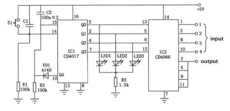
Introduction to the CD4066 IC
The CD4066 is a quad bilateral switch integrated circuit (IC) that is commonly used in analog and mixed-signal applications. This versatile IC, also known as the 4066 or HEF4066, is part of the 4000 series of CMOS logic ICs. It is designed to switch or multiplex analog or digital signals, making it a valuable component in a wide range of electronic circuits.
Key Features of the CD4066
The CD4066 has several notable features that make it an attractive choice for various applications:
-
Quad bilateral switches: The CD4066 contains four independent bilateral switches, allowing for multiple signal routing options within a single IC package.
-
Low on-resistance: When the switches are closed, they exhibit a low on-resistance, typically around 50-100 ohms, which minimizes signal attenuation and ensures efficient signal transmission.
-
High off-resistance: In the open state, the switches have a high off-resistance, typically in the range of several gigaohms, providing excellent isolation between the input and output.
-
Wide supply voltage range: The CD4066 can operate with a supply voltage ranging from 3V to 15V, making it compatible with various power supply configurations.
-
Low power consumption: As a CMOS device, the CD4066 has low static power consumption, making it suitable for battery-powered applications.
-
High switching speed: The CD4066 can switch signals at frequencies up to several MHz, allowing for fast signal routing and multiplexing.

CD4066 Pin Configuration and Function Table
The CD4066 is available in several package types, including DIP (Dual In-line Package), SO (Small Outline), and TSSOP (Thin-Shrink Small Outline Package). The following table shows the pin configuration and functions for a 14-pin DIP package:
| Pin Number | Pin Name | Function |
|---|---|---|
| 1 | 1IN/1OUT | Switch 1 input/output |
| 2 | 1OUT/1IN | Switch 1 output/input |
| 3 | 1CONTROL | Switch 1 control input |
| 4 | 2IN/2OUT | Switch 2 input/output |
| 5 | 2OUT/2IN | Switch 2 output/input |
| 6 | 2CONTROL | Switch 2 control input |
| 7 | VSS | Ground (0V) |
| 8 | 3CONTROL | Switch 3 control input |
| 9 | 3OUT/3IN | Switch 3 output/input |
| 10 | 3IN/3OUT | Switch 3 input/output |
| 11 | 4CONTROL | Switch 4 control input |
| 12 | 4OUT/4IN | Switch 4 output/input |
| 13 | 4IN/4OUT | Switch 4 input/output |
| 14 | VDD | Positive supply voltage |

Working Principle of the CD4066
The CD4066 contains four bilateral switches, each consisting of a pair of complementary MOS transistors (NMOS and PMOS) connected in parallel. The control input of each switch is connected to the gates of these transistors.
When a logic high (typically VDD) is applied to the control input, the NMOS and PMOS transistors are turned on, creating a low-resistance path between the input and output terminals of the switch. This allows the signal to pass through the switch with minimal attenuation.
Conversely, when a logic low (typically VSS or ground) is applied to the control input, both transistors are turned off, resulting in a high-resistance path between the input and output terminals. This effectively isolates the input from the output, preventing the signal from passing through the switch.
The bilateral nature of the switches allows signals to flow in either direction when the switch is closed, making the CD4066 suitable for bidirectional signal routing and multiplexing applications.

CD4066 Characteristics
DC Characteristics
The following table summarizes the key DC characteristics of the CD4066:
| Parameter | Symbol | Min | Typ | Max | Unit |
|---|---|---|---|---|---|
| Supply Voltage | VDD | 3 | – | 15 | V |
| Input Voltage | VIN | 0 | – | VDD | V |
| Input Leakage Current | IIN | – | – | 1 | µA |
| Output Leakage Current | IOUT | – | – | 1 | µA |
| On-Resistance (VDD=5V, RL=1kΩ) | RON | – | 50 | 100 | Ω |
| Off-Resistance (VDD=5V, RL=1MΩ) | ROFF | 1000 | – | – | MΩ |
AC Characteristics
The following table summarizes the key AC characteristics of the CD4066:
| Parameter | Symbol | Min | Typ | Max | Unit |
|---|---|---|---|---|---|
| Propagation Delay (CL=50pF) | tPD | – | 60 | 150 | ns |
| Transition Time (CL=50pF) | tt | – | 80 | 200 | ns |
| Maximum Toggle Frequency | fMAX | – | 5 | – | MHz |
These characteristics demonstrate the CD4066’s ability to switch signals quickly and efficiently, making it suitable for a wide range of applications.
Applications of the CD4066
The CD4066 finds use in various analog and mixed-signal applications, including:
-
Analog signal multiplexing: The CD4066 can be used to select one of several analog input signals and route it to a single output, such as in data acquisition systems or analog front-ends.
-
Sample-and-hold circuits: By using a switch to control the charging and discharging of a capacitor, the CD4066 can be used to create sample-and-hold circuits for analog signal processing.
-
Analog signal gating: The CD4066 can be used to gate or chop analog signals, which is useful in applications such as lock-in amplifiers or synchronous demodulators.
-
Voltage-controlled resistors: By using the CD4066 as a variable resistor, it is possible to create voltage-controlled filters, amplifiers, or oscillators.
-
Digital signal routing: Although primarily designed for analog signals, the CD4066 can also be used to route digital signals, such as in multiplexers or demultiplexers.
-
Audio and video switching: The CD4066’s low on-resistance and high off-resistance make it suitable for switching audio and video signals in consumer electronics devices.
Interfacing the CD4066 with Microcontrollers
The CD4066 can be easily interfaced with microcontrollers to enable software control of analog signal routing. To control the switches, the microcontroller’s digital output pins can be connected to the control inputs of the CD4066.
When using the CD4066 with microcontrollers, consider the following:
-
Logic level compatibility: Ensure that the microcontroller’s digital output levels are compatible with the CD4066’s control input requirements. If necessary, use level shifters to match the voltage levels.
-
Switching speed: The CD4066’s switching speed may be limited by the microcontroller’s digital output rise and fall times. If faster switching is required, consider using a microcontroller with faster GPIO capabilities or external driver circuits.
-
Analog signal considerations: When routing analog signals, pay attention to the CD4066’s on-resistance and its impact on signal integrity. Also, ensure proper grounding and shielding techniques to minimize noise and crosstalk.
By combining the flexibility of the CD4066 with the programmability of microcontrollers, designers can create highly adaptable and reconfigurable analog signal processing systems.
CD4066 Application Circuits
Simple Analog Multiplexer
One of the most common applications of the CD4066 is as an analog multiplexer. The following schematic shows a simple 4-to-1 analog multiplexer using a single CD4066 IC:
         +---------+
IN0 -----|1IN/1OUT |
         |         |
IN1 -----|2IN/2OUT |
         |         |
IN2 -----|3IN/3OUT |
         |         |
IN3 -----|4IN/4OUT |
         |         |
S0 ------|1CONTROL |
         |         |
S1 ------|2CONTROL |
         |         |
    VSS--|   VSS   |
         |         |
    VDD--|   VDD   |
         |         |
         |3CONTROL |
         |         |
         |4CONTROL |
         |         |
         |1OUT/1IN |---- OUT
         |         |
         |2OUT/2IN |
         |         |
         |3OUT/3IN |
         |         |
         |4OUT/4IN |
         +---------+
In this circuit, the four analog input signals (IN0, IN1, IN2, and IN3) are connected to the input/output pins of the CD4066’s switches. The control inputs (S0 and S1) are used to select which input signal is routed to the output (OUT). By applying the appropriate logic levels to S0 and S1, any one of the four input signals can be selected and passed to the output.
Voltage-Controlled Resistor
Another useful application of the CD4066 is as a voltage-controlled resistor. By connecting a potentiometer or a digital-to-analog converter (DAC) to the control input of a switch, the on-resistance of the switch can be varied, effectively creating a variable resistor. This technique can be used to create voltage-controlled filters, amplifiers, or oscillators.
The following schematic shows a simple voltage-controlled resistor using a single switch of the CD4066:
         +---------+
IN ------| 1IN/1OUT|--+------ OUT
         |         |  |
CTRL -+--|1CONTROL |  |
      |  |         |  |
     GND-|   VSS   |  |
         |         |  |
     VDD-|   VDD   |  |
         |         |  |
         |1OUT/1IN |--+
         |         |
         | 2,3,4   |
         | (NC)    |
         +---------+
In this circuit, the input signal (IN) is connected to one terminal of the switch, while the output (OUT) is connected to the other terminal. The control voltage (CTRL) is applied to the control input of the switch, varying its on-resistance. As the control voltage changes, the resistance between IN and OUT changes, allowing for voltage-controlled signal attenuation or filtering.
CD4066 vs. Other Analog Switch ICs
While the CD4066 is a popular choice for analog switching applications, there are other analog switch ICs available, each with its own unique features and characteristics. Some common alternatives include:
-
CD4051/CD4052/CD4053: These are single 8-channel, differential 4-channel, and triple 2-channel analog multiplexers, respectively. They offer more switching channels than the CD4066 but have a slightly higher on-resistance.
-
ADG1411/ADG1412: These are modern, low-voltage, low-power analog switches with a single SPST (ADG1411) or SPDT (ADG1412) configuration. They offer lower on-resistance and faster switching speeds than the CD4066 but have fewer channels.
-
DG419/DG441/DG442: These are high-performance, low-voltage, CMOS analog switches with various configurations, including SPST, SPDT, and DPDT. They provide lower on-resistance, faster switching speeds, and lower leakage currents compared to the CD4066.
When selecting an analog switch IC, consider factors such as the number of channels required, on-resistance, switching speed, power consumption, and supply voltage compatibility. The CD4066 remains a popular choice due to its simplicity, versatility, and wide availability, but other options may be more suitable for specific applications or performance requirements.
FAQs
-
What is the maximum supply voltage for the CD4066?
The CD4066 can operate with a supply voltage ranging from 3V to 15V, making it compatible with a wide range of power supply configurations. -
How many channels does the CD4066 have?
The CD4066 contains four independent bilateral switches, allowing for up to four separate signal routing or multiplexing channels. -
What is the typical on-resistance of the CD4066’s switches?
The CD4066’s switches have a typical on-resistance of around 50-100 ohms when the supply voltage is 5V and the load resistance is 1 kΩ. -
Can the CD4066 be used for digital signal routing?
Although primarily designed for analog signals, the CD4066 can also be used to route digital signals, such as in multiplexers or demultiplexers. However, its switching speed may be lower than dedicated digital switching ICs. -
How can I control the CD4066’s switches using a microcontroller?
To control the CD4066’s switches with a microcontroller, connect the microcontroller’s digital output pins to the control inputs of the CD4066. Ensure that the logic levels are compatible and consider the switching speed limitations imposed by the microcontroller’s GPIO capabilities.
Conclusion
The CD4066 quad bilateral switch is a versatile and widely-used IC in analog and mixed-signal applications. Its key features, such as low on-resistance, high off-resistance, and wide supply voltage range, make it suitable for a variety of signal routing, multiplexing, and processing tasks.
By understanding the CD4066’s working principle, characteristics, and application circuits, designers can effectively incorporate this IC into their projects. Whether used as an analog multiplexer, voltage-controlled resistor, or signal gating element, the CD4066 offers flexibility and performance in a compact package.
As with any electronic component, it is essential to consider the specific requirements of the application and compare the CD4066 with other available analog switch ICs to select the most appropriate solution. By leveraging the capabilities of the CD4066 and following best design practices, engineers can create robust, efficient, and adaptable analog signal processing systems.


Leave a Reply