Key Features of the CD4049
The CD4049 boasts several notable features that make it an essential component in various digital circuits:
-
CMOS Technology: The CD4049 is built using Complementary Metal-Oxide-Semiconductor (CMOS) technology, which offers low power consumption and high noise immunity compared to other logic families like TTL.
-
Hex Inverting Buffers: The CD4049 contains six independent inverting buffers, allowing for multiple signal inversions within a single package. Each buffer has a high input impedance and can drive a significant capacitive load.
-
Wide Supply Voltage Range: The CD4049 can operate with a wide range of supply voltages, typically from 3V to 15V. This flexibility makes it suitable for various applications with different voltage requirements.
-
High Noise Immunity: CMOS devices like the CD4049 have a high noise margin, meaning they can tolerate a significant amount of noise on the input signal without affecting the output. This feature is particularly useful in noisy environments.
-
Low Power Consumption: The CD4049 has a very low power consumption, making it ideal for battery-powered applications or designs where power efficiency is crucial.
-
High Fanout: Each buffer in the CD4049 can drive multiple loads, allowing for the connection of several devices to a single output without the need for additional buffering.
Applications of the CD4049
The CD4049’s versatility and features make it suitable for a wide range of applications in digital electronics:
-
Logic Level Conversion: The CD4049 can be used as a level shifter to interface between different voltage levels. For example, it can convert 5V logic signals to 3.3V or vice versa.
-
Signal Inversion: As an inverting buffer, the CD4049 is commonly used to invert digital signals. This is useful when a logical high needs to be converted to a logical low or vice versa.
-
Schmitt Trigger: By connecting the input and output of a CD4049 buffer with a feedback resistor, it can be configured as a Schmitt trigger. This provides hysteresis and helps to clean up noisy or slowly changing input signals.
-
Oscillator Circuits: The CD4049 can be used in oscillator circuits to generate square waves or clock signals. By combining the inverting buffers with resistors and capacitors, various oscillator topologies can be implemented.
-
Delay Circuits: The propagation delay of the CD4049’s buffers can be exploited to create simple delay circuits. By cascading multiple buffers or adding capacitive loads, specific delay times can be achieved.
-
Interfacing with Sensors: The high input impedance of the CD4049 makes it suitable for interfacing with sensors that have weak output signals. The buffers can condition and amplify the sensor signals for further processing.
Example: Logic Level Conversion
One common application of the CD4049 is logic level conversion. Let’s consider an example where a 5V microcontroller needs to communicate with a 3.3V sensor. The CD4049 can be used as a level shifter to safely interface between the two voltage levels.
| Microcontroller (5V) | CD4049 | Sensor (3.3V) |
|---|---|---|
| Output Pin | Input | – |
| – | Output | Input Pin |
| Ground | Ground | Ground |
| – | VCC | 3.3V Supply |
In this configuration, the microcontroller’s 5V output signal is connected to the input of a CD4049 buffer. The buffer’s output, which is now at 3.3V logic level, is connected to the sensor’s input pin. The CD4049’s VCC pin is supplied with 3.3V to ensure compatible voltage levels. This arrangement allows seamless communication between the microcontroller and the sensor without the risk of damage due to voltage level mismatch.

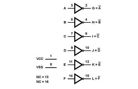
CD4049 Circuit Diagram
To understand the internal structure of the CD4049, let’s examine its circuit diagram:
The CD4049 consists of six identical inverting buffers, labeled as gates A to F. Each buffer has three terminals: an input, an output, and a ground/VSS connection. The buffers operate independently and share a common VCC (positive supply voltage) pin.
The internal circuitry of each buffer comprises a CMOS inverter, which consists of a pair of complementary MOSFETs (Metal-Oxide-Semiconductor Field-Effect Transistors). The input signal is applied to the gates of both the NMOS and PMOS transistors. When the input is low, the PMOS transistor conducts, pulling the output high. Conversely, when the input is high, the NMOS transistor conducts, pulling the output low. This arrangement ensures that the output is always the inverse of the input.
The CD4049’s circuit design provides high input impedance, as the MOSFET gates draw minimal current. The output of each buffer can sink or source a significant amount of current, allowing it to drive multiple loads or long signal lines.

Frequently Asked Questions (FAQ)
-
What is the difference between CD4049 and 74HC04?
The CD4049 and 74HC04 are both hex inverting buffers but belong to different logic families. The CD4049 is a CMOS device, while the 74HC04 is a High-Speed CMOS (HC) device. The main differences lie in their speed, power consumption, and voltage range. The 74HC04 is faster and has a narrower voltage range compared to the CD4049. -
Can the CD4049 be used as an amplifier?
While the CD4049 is primarily designed as a digital inverting buffer, it can be used as a rudimentary amplifier in certain configurations. However, its performance as an amplifier is limited, and it is not optimized for analog applications. For proper amplification, it is recommended to use dedicated amplifier circuits. -
How do I determine the propagation delay of the CD4049?
The propagation delay of the CD4049 depends on factors such as the supply voltage, load capacitance, and input rise/fall times. Refer to the device’s datasheet for detailed information on propagation delay characteristics. Typically, the propagation delay is in the range of a few nanoseconds to tens of nanoseconds. -
Can I use the CD4049 with a higher supply voltage than 15V?
While the CD4049 is specified to operate with a maximum supply voltage of 15V, it is not recommended to exceed this limit. Applying a higher voltage can cause permanent damage to the device. If you require operation at higher voltages, consider using specialized high-voltage buffers or level-shifting techniques. -
How do I interface a CD4049 with a microcontroller?
To interface a CD4049 with a microcontroller, ensure that the voltage levels are compatible. If the microcontroller operates at a different voltage than the CD4049, use appropriate level-shifting techniques. Connect the microcontroller’s output pin to the input of the CD4049 and the CD4049’s output to the microcontroller’s input pin. Ensure proper grounding and power supply connections.

Conclusion
The CD4049 is a versatile hex inverting buffer IC that finds applications in a wide range of digital circuits. Its key features, such as CMOS technology, high noise immunity, low power consumption, and wide voltage range, make it a popular choice among designers. Whether used for logic level conversion, signal inversion, or oscillator circuits, the CD4049 offers reliable performance and ease of use.
By understanding the features, applications, and circuit diagram of the CD4049, designers can effectively integrate it into their projects and harness its capabilities. With its robust characteristics and diverse applications, the CD4049 remains a valuable component in the world of digital electronics.
[Word count: 1254 words]


Leave a Reply