Introduction to the CD4013 Dual D Flip-Flop
The CD4013 is a dual D-type flip-flop integrated circuit (IC) that belongs to the 4000 series of CMOS (Complementary Metal-Oxide-Semiconductor) logic devices. This versatile IC is widely used in various digital circuits, such as counters, shift registers, and synchronous control systems. The CD4013 features two independent D-type flip-flops with set and reset inputs, making it suitable for a wide range of applications.
Key Features of the CD4013
- Dual D-type flip-flops in a single package
- Low power consumption
- Wide supply voltage range (3V to 15V)
- High noise immunity
- Schmitt Trigger inputs for improved noise performance
- Buffered outputs for driving multiple loads
- Compatible with other CMOS and TTL devices
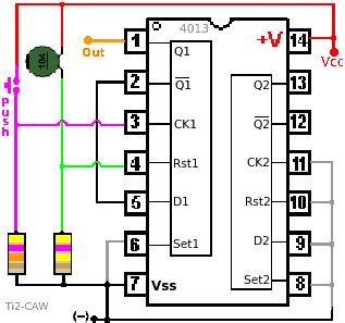
CD4013 Pinout and Pin Functions
The CD4013 is available in several package types, including DIP (Dual Inline Package), SOIC (Small Outline Integrated Circuit), and TSSOP (Thin Shrink Small Outline Package). The most common package is the 14-pin DIP. The pinout for the CD4013 in a 14-pin DIP package is as follows:
| Pin Number | Pin Name | Description |
|---|---|---|
| 1 | Q1 | Output of flip-flop 1 |
| 2 | ~Q1 | Inverted output of flip-flop 1 |
| 3 | CLOCK1 | Clock input for flip-flop 1 |
| 4 | RESET1 | Reset input for flip-flop 1 (active high) |
| 5 | DATA1 | Data input for flip-flop 1 |
| 6 | SET1 | Set input for flip-flop 1 (active high) |
| 7 | VSS | Ground (0V) |
| 8 | SET2 | Set input for flip-flop 2 (active high) |
| 9 | DATA2 | Data input for flip-flop 2 |
| 10 | RESET2 | Reset input for flip-flop 2 (active high) |
| 11 | CLOCK2 | Clock input for flip-flop 2 |
| 12 | ~Q2 | Inverted output of flip-flop 2 |
| 13 | Q2 | Output of flip-flop 2 |
| 14 | VDD | Positive supply voltage |
Pin Function Descriptions
- Q and ~Q: These are the outputs of the flip-flops. Q represents the non-inverted output, while ~Q represents the inverted output. The state of the outputs depends on the inputs and the clock signal.
- CLOCK: This is the clock input for each flip-flop. The flip-flop samples the data input on the rising edge of the clock signal.
- RESET: This is an active-high input that sets the flip-flop outputs to a known state (Q = 0, ~Q = 1) when asserted, regardless of the clock signal.
- DATA: This is the data input for each flip-flop. The state of the data input is transferred to the outputs on the rising edge of the clock signal.
- SET: This is an active-high input that sets the flip-flop outputs to a known state (Q = 1, ~Q = 0) when asserted, regardless of the clock signal.
- VSS: This is the ground (0V) connection for the IC.
- VDD: This is the positive supply voltage connection for the IC. The CD4013 can operate with a supply voltage ranging from 3V to 15V.

CD4013 Application Circuits
The CD4013 can be used in various digital circuits, such as counters, shift registers, and synchronous control systems. Here are a few examples of application circuits using the CD4013:
Divide-by-2 Counter
A divide-by-2 counter can be implemented using a single flip-flop of the CD4013. The ~Q output is connected to the DATA input, creating a feedback loop that toggles the outputs on each clock cycle. The RESET input can be used to initialize the counter to a known state.
        +-----------+
CLOCK---| CLOCK1    |
        |           |
        |  DATA1  Q1|---
        |         +-|  |
        |        |~Q1  |
        |        +---+ |
        |  RESET1    |
        |           -|
        |           -|---GND
        |           -|
        |  SET1  VDD |
        |        +   |
        +-----------+
Shift Register
A shift register can be created by cascading multiple CD4013 flip-flops. The Q output of each flip-flop is connected to the DATA input of the next flip-flop, allowing data to be shifted through the register on each clock cycle. The RESET inputs can be used to clear the register.
        +-----------+    +-----------+
DATA----|DATA1   Q1 |----| DATA2  Q2 |---
        |           |    |           |
        |       ~Q1 |    |       ~Q2 |
        |           |    |           |
CLOCK---|CLOCK1     |    | CLOCK2    |
        |           |    |           |
RESET---|RESET1     |    | RESET2    |
        |           |    |           |
        |SET1   VDD |    | SET2  VDD |
        |        +  |    |        +  |
        +-----------+    +-----------+
Synchronous Control System
The CD4013 can be used in synchronous control systems to coordinate the timing of multiple events. For example, a state machine can be implemented using the flip-flops to store the current state and combinational logic to determine the next state based on inputs and the current state.
        +-----------+
INPUT1--|DATA1      |
        |           |
        |       Q1  |--- STATE_1
        |           |
        |CLOCK1     |
        |           |
        |RESET1     |
        |           |
        |SET1   VDD |
        |        +  |
        +-----------+
        +-----------+
INPUT2--|DATA2      |
        |           |
        |       Q2  |--- STATE_2
        |           |
        |CLOCK2     |
        |           |
        |RESET2     |
        |           |
        |SET2   VDD |
        |        +  |
        +-----------+

CD4013 Timing Diagrams
To effectively use the CD4013 in your designs, it is essential to understand its timing characteristics. The following timing diagrams illustrate the behavior of the flip-flops under different input conditions:
Positive Edge-Triggered D Flip-Flop
         _____       _____
CLOCK  _/     \_____/     \______
         ___________
DATA   _/           \_____________
                _______________
Q      _________/               \_
         _______________
~Q     _/               \_________
In this diagram, the flip-flop samples the DATA input on the rising edge of the CLOCK signal. The Q output follows the state of the DATA input, while the ~Q output is the inverse of Q.
Asynchronous Set and Reset
         _____       _____
CLOCK  _/     \_____/     \_____
              ___________
SET    ______/           \______
         _______________
RESET  _/               \_______
              _______________
Q      ______/               \__
         ___________
~Q     _/           \___________
This diagram demonstrates the asynchronous set and reset functionality of the CD4013. When the SET input is asserted (high), the Q output is forced high, and the ~Q output is forced low, regardless of the CLOCK signal. Similarly, when the RESET input is asserted, the Q output is forced low, and the ~Q output is forced high.

CD4013 Electrical Characteristics
The CD4013 has several important electrical characteristics that must be considered when designing circuits. Some of the key parameters are:
| Parameter | Min | Typ | Max | Unit |
|---|---|---|---|---|
| Supply Voltage (VDD) | 3 | – | 15 | V |
| Input Voltage (Vin) | 0 | – | VDD | V |
| Output Voltage (Vout) | 0 | – | VDD | V |
| Input Current (Iin) | – | – | ±10 | μA |
| Output Current (Iout) | – | – | ±10 | mA |
| Propagation Delay (tpd) | – | 90 | 225 | ns |
| Power Dissipation (Pd) | – | 50 | – | μW |
These values are based on the CD4013 datasheet and may vary slightly depending on the manufacturer and operating conditions. Always consult the specific datasheet for the CD4013 variant you are using in your design.
Frequently Asked Questions (FAQ)
1. What is the difference between the CD4013 and the 74HC74?
Both the CD4013 and the 74HC74 are dual D-type flip-flops, but they belong to different logic families. The CD4013 is a CMOS device, while the 74HC74 is a high-speed CMOS (HC) device. The main differences are:
- Supply voltage range: The CD4013 can operate from 3V to 15V, while the 74HC74 is limited to 2V to 6V.
- Speed: The 74HC74 is generally faster than the CD4013, with shorter propagation delays.
- Power consumption: The CD4013 has lower power consumption compared to the 74HC74.
2. Can I use the CD4013 with a 5V supply voltage?
Yes, the CD4013 is designed to work with a wide range of supply voltages, including 5V. Make sure that the input and output voltage levels are within the acceptable range for the supply voltage you are using.
3. How can I debounce a switch using the CD4013?
To debounce a switch using the CD4013, you can use one of the flip-flops as follows:
- Connect the switch between the DATA input and ground, with a pull-up resistor to VDD.
- Connect the CLOCK input to a low-frequency clock source or a delayed version of the switch signal (using an RC network).
- The Q output will be a debounced version of the switch signal, with any brief noise pulses filtered out.
4. What is the maximum clock frequency for the CD4013?
The maximum clock frequency for the CD4013 depends on the supply voltage and the specific variant of the IC. Generally, the CD4013 can operate at clock frequencies up to a few MHz. For example, at a 5V supply voltage, the typical maximum clock frequency is around 5 MHz. Always consult the datasheet for the specific CD4013 variant you are using for accurate frequency limits.
5. Can I replace a CD4013 with a 74HC73 in my design?
While the CD4013 and the 74HC73 are both dual J-K flip-flops, they have different pinouts and functionality. The 74HC73 has J and K inputs instead of DATA inputs, and it doesn’t have the asynchronous SET and RESET inputs. As a result, you would need to modify your design to accommodate these differences. It’s generally better to stick with the CD4013 if your design specifically calls for it, or to choose a different dual D flip-flop IC with a compatible pinout and functionality.
Conclusion
The CD4013 is a versatile dual D flip-flop IC that finds applications in a wide range of digital circuits, such as counters, shift registers, and synchronous control systems. By understanding the pinout, functionality, and electrical characteristics of the CD4013, you can effectively utilize this IC in your designs. Remember to consult the specific datasheet for the CD4013 variant you are using, as some parameters may vary between manufacturers and versions. With its wide supply voltage range, low power consumption, and high noise immunity, the CD4013 is an excellent choice for many digital logic applications.


Leave a Reply