ALL ABOUT FLEX PCB
-
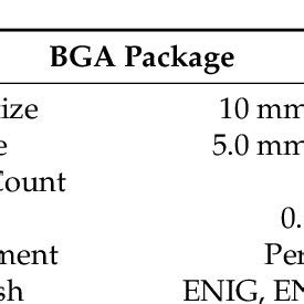
Read more: ENEPIG vs. ENIG: Which is the Better Surface Finish?
What is ENEPIG? ENEPIG, short for Electroless Nickel Electroless Palladium Immersion Gold, is a multi-layer surface finish that consists of three distinct layers: Electroless Nickel (Ni): This layer acts as a barrier between the copper substrate and the subsequent layers, providing excellent corrosion resistance and a uniform surface for the […]
-
 Read more: A Guide of Moving from Breadboard PCB Prototypes to Full Product
Finalize and Test Your Breadboard Prototype Before starting the process of creating a PCB version of your project, make sure your breadboard prototype is fully complete, tested, and working as intended. Iron out any remaining bugs and validate that it meets all of your design requirements and specifications. Key Points […]
-
Optimize High Current PCB for Motor Controls
Posted by
–
 Read more: Optimize High Current PCB for Motor Controls
Introduction to PCB Optimization for High Current Motor Control Applications Printed Circuit Boards (PCBs) are essential components in modern electronics, providing a platform for interconnecting electronic components and ensuring reliable operation. When it comes to high current motor control applications, PCB optimization becomes crucial to ensure efficient power delivery, minimize […]
-
Outsource DFM Service to RAYMING
Posted by
–
 Read more: Outsource DFM Service to RAYMING
What is Design for Manufacturability (DFM)? Design for Manufacturability (DFM) is the practice of designing products in a way that makes them easier, faster, and more cost-effective to manufacture. DFM involves considering various aspects of the manufacturing process during the design phase, such as material selection, part geometry, tolerances, and […]
-
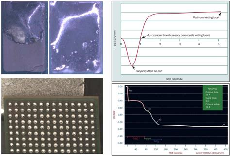 Read more: Solderability Test: Understanding PCB Solderability Testing
What is Solderability Testing? Solderability testing is a process used to evaluate the ability of electronic components and printed circuit boards (PCBs) to be soldered effectively. It assesses the wettability and adhesion properties of the surfaces to be soldered, ensuring reliable electrical connections and mechanical strength. Solderability testing is crucial […]
-
When should I choose 2 layer PCB or 4 layer PCB
Posted by
–
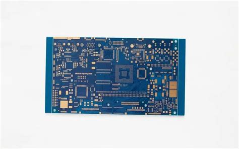 Read more: When should I choose 2 layer PCB or 4 layer PCB
Understanding PCB Layers Before diving into the comparison between 2 layer and 4 layer PCBs, let’s first understand what PCB layers are and their significance. What are PCB Layers? PCB layers refer to the number of conductive copper layers within a PCB. These layers are used to route electrical signals […]
-
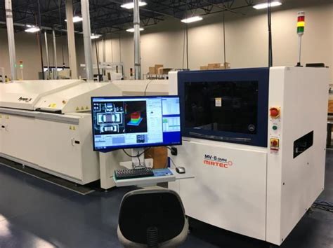
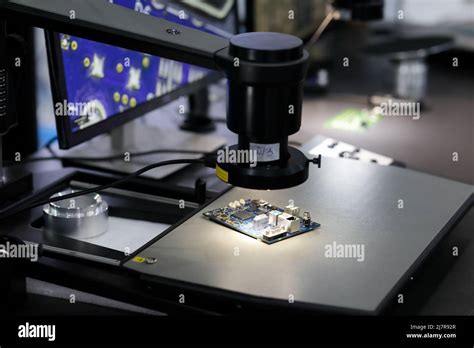
The Final Inspection of PCB Assembly
Posted by
–
 Read more: The Final Inspection of PCB Assembly
Introduction to PCB inspection Printed Circuit Board (PCB) assembly is a complex process involving many steps, from component placement to soldering. To ensure the quality and reliability of the final product, a thorough inspection is crucial. This final inspection is the last line of defense against any defects or issues […]
-
What is x-ray inspection in PCB?
Posted by
–
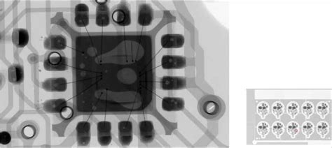 Read more: What is x-ray inspection in PCB?
What is a Printed Circuit Board (PCB)? A printed circuit board, or PCB, is a fundamental component in modern electronic devices. It is a flat board made of insulating materials, such as fiberglass or composite epoxy, with conductive pathways etched or printed onto its surface. These pathways, known as traces, […]
-
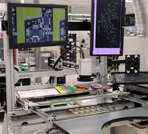
 Read more: The Most Detailed Introduction AOI Inspection(Latest)
What is AOI Inspection? AOI (Automated Optical Inspection) is a critical process in the manufacturing of printed circuit boards (PCBs) and other electronic components. It involves using specialized cameras and image processing software to automatically inspect the quality of manufactured products for defects, such as missing components, incorrect component placement, […]
-
What is the PCB incoming inspection process?
Posted by
–
 Read more: What is the PCB incoming inspection process?
Introduction to PCB inspection Printed Circuit Board (PCB) inspection is a crucial step in ensuring the quality and reliability of electronic products. The PCB incoming inspection process is designed to identify and eliminate defects, anomalies, and non-conformities in the PCBs before they are used in the manufacturing process. This comprehensive […]


