
ALL ABOUT FLEX PCB
-
Read more: High Power LED Lights with 100W, 200W, and Higher Power
What are High Power LED Lights? High power LED lights are a type of light-emitting diode (LED) technology designed to deliver exceptional brightness and efficiency. These lights typically have power ratings of 100W, 200W, and higher, making them suitable for a wide range of applications that require intense illumination. Some key characteristics of high power…
-
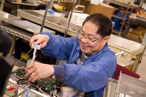
6 Tips on How To Repair Printed Circuit Board
Posted by
–
 Read more: 6 Tips on How To Repair Printed Circuit Board
Understanding PCB Repair PCB repair is the process of identifying and fixing issues in a printed circuit board to restore its functionality. This can involve various techniques, such as soldering, desoldering, cleaning, and replacing components. Successful PCB repair requires a combination of technical knowledge, practical skills, and the right tools. Common PCB Issues Before diving…
-
WHAT ARE GOLD FINGERS
Posted by
–
 Read more: WHAT ARE GOLD FINGERS
Introduction to Gold Fingers Gold fingers, also known as edge connectors, are a type of electrical connector commonly found on printed circuit boards (PCBs) and various electronic devices. These connectors are named “gold fingers” due to the gold-plated contacts that protrude from the edge of the PCB, resembling fingers. Gold fingers play a crucial role…
-
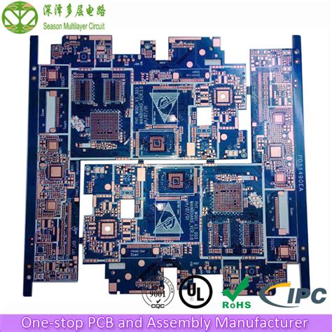
HDI PCB High Density Interconnect PCB
Posted by
–
 Read more: HDI PCB High Density Interconnect PCB
What is HDI PCB? HDI PCB is a type of printed circuit board that features higher wiring density per unit area compared to conventional PCBs. This increased density is achieved through the use of smaller vias, finer trace widths and spaces, and multiple layers of interconnections. The result is a compact, high-performance board that can…
-
What is PCB File
Posted by
–
 Read more: What is PCB File
What Does PCB Stand For? PCB stands for Printed Circuit Board. A PCB File contains all the data needed to design and manufacture a printed circuit board, including the schematic, component layout, trace routing, drill holes, and other specifications. PCB files allow designers to digitally create and share Circuit Board Designs that can then be…
-
What is PCB Copper Layers
Posted by
–
 Read more: What is PCB Copper Layers
What are PCB Copper Layers? PCB copper layers are thin sheets of copper foil laminated onto the insulating substrate material of a printed circuit board. These layers act as conductive pathways for electrical signals and power distribution between various components on the board. The number of copper layers in a PCB can vary depending on…
-
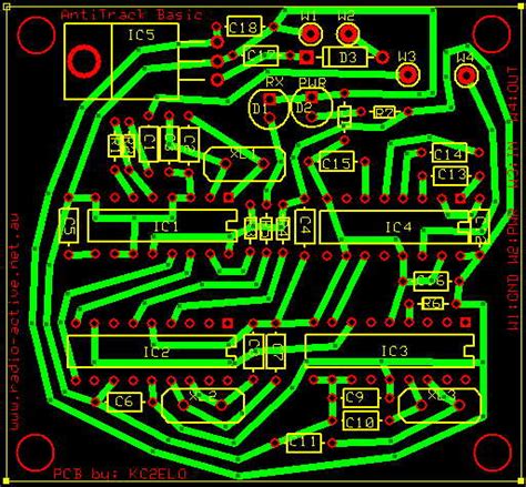
Why is track width important in PCB design?
Posted by
–
 Read more: Why is track width important in PCB design?
Introduction to Track width in PCB Design Track width is a crucial aspect of printed circuit board (PCB) design that significantly impacts the performance, reliability, and manufacturability of electronic devices. In PCB design, tracks are the conductive paths that carry electrical signals and power between components. The width of these tracks plays a vital role…
-
 Read more: 11 Effective Ways to Cut PCB Assembly Cost Without Sacrificing Quality
1. Optimize PCB Design for Manufacturing (DFM) One of the most effective ways to cut PCB Assembly Costs is to optimize your PCB design for manufacturing (DFM). By following DFM guidelines, you can ensure that your PCB design is compatible with the manufacturing process, minimizing the risk of errors, delays, and additional costs. Some key…
-
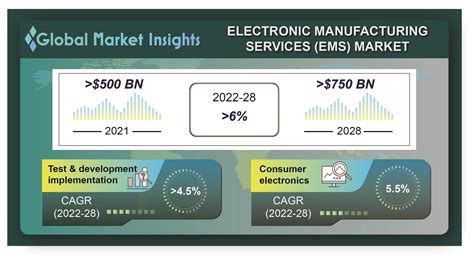 Read more: Electronic Manufacturing Services (EMS) Market Analysis & Trends 2024
Overview of the EMS Market Electronic Manufacturing Services (EMS) refers to the outsourcing of electronic product manufacturing to specialized companies. These companies provide a range of services, including design, assembly, testing, and supply chain management. The EMS industry has grown significantly over the past few decades, driven by the increasing complexity of electronic devices and…
-
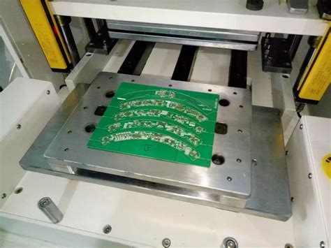
 Read more: Pay attention to some issues related to Express PCB manufacturing & assembly.
What is Express PCB Manufacturing? Express PCB manufacturing refers to the rapid fabrication and assembly of printed circuit boards (PCBs) within a short turnaround time. This service is essential for businesses and individuals who require quick prototyping or small-scale production of PCBs for their projects. Express PCB manufacturers utilize advanced technology and streamlined processes to…


