ALL ABOUT FLEX PCB
-
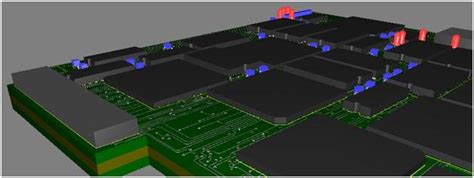
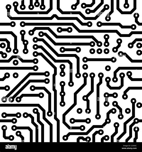
Copper fills – mechanically speaking
Posted by
–
Read more: Copper fills – mechanically speakingIntroduction to Copper fills Copper fills, also known as copper vias or PTHs (plated through holes), are a crucial component in printed circuit boards (PCBs). They provide electrical connections between different layers of a multi-layer PCB, enabling the flow of signals and power throughout the board. From a mechanical perspective, copper fills play a significant…
-
 Read more: 7 FAQs about PCB Assembly Services You Don’t Want to Miss
What is PCB Assembly? PCB assembly is the process of attaching electronic components to a printed circuit board. The process involves several steps, including: Solder Paste Application: A thin layer of solder paste is applied to the PCB’s contact pads using a stencil or screen printing process. Component Placement: The electronic components are precisely placed…
-
Hot PCB FPGA MCU News From Altium
Posted by
–
 Read more: Hot PCB FPGA MCU News From Altium
Altium Unveils Cutting-Edge PCB Design Tools and Features Altium, a leading provider of electronic design automation software, has recently announced a series of exciting updates and new features for their PCB design tools. These updates aim to streamline the design process, enhance productivity, and facilitate innovation in the world of printed circuit boards (PCBs), field-programmable…
-
What is track width (TW)?
Posted by
–
 Read more: What is track width (TW)?
Importance of Track width The track width of a vehicle has a significant impact on its handling and stability. A wider track width generally provides better stability and handling, especially during cornering and high-speed maneuvers. This is because a wider track width reduces the vehicle’s tendency to roll and increases its resistance to lateral forces.…
-
The Optimum PCB Design Flow – Right First Time
Posted by
–
 Read more: The Optimum PCB Design Flow – Right First Time
Introduction Designing a printed circuit board (PCB) can be a complex and time-consuming process, with many steps and potential pitfalls along the way. Getting the PCB design right the first time is critical to avoid costly redesigns, manufacturing delays, and product failures. In this article, we’ll explore the optimum PCB Design Flow to help you…
-
cEDM – Electronics Design & Manufacturing
Posted by
–
 Read more: cEDM – Electronics Design & Manufacturing
Introduction to cEDM cEDM, or Collaborative Electronic Design and Manufacturing, is a groundbreaking approach that combines the power of collaborative design with the efficiency of modern manufacturing techniques. This innovative methodology is transforming the way electronics are designed and produced, enabling companies to bring their products to market faster, more cost-effectively, and with higher quality…
-
Review – Standard and Predefined Build-ups
Posted by
–
 Read more: Review – Standard and Predefined Build-ups
What are Build-ups? Build-ups, in the context of construction and engineering, refer to the process of gradually increasing the complexity or size of a structure or system. This approach is commonly used in various fields, such as software development, manufacturing, and project management. The main purpose of build-ups is to ensure that the final product…
-
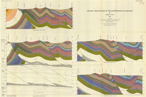
Cross Sections – What is their Purpose ?
Posted by
–
 Read more: Cross Sections – What is their Purpose ?
What are Cross Sections? A cross section is a view of an object as if it had been sliced through to reveal its internal structure. Imagine cutting a loaf of bread in half and looking at the exposed surface – this is essentially a cross section. Cross sections can be taken along any plane, but…
-
What are specific markings?
Posted by
–
 Read more: What are specific markings?
Types of Specific markings There are various types of specific markings used across different industries and applications. Some of the most common categories include: Security Classification Markings Security classification markings indicate the level of sensitivity and protective measures required for information or assets. Examples include: UNCLASSIFIED CONFIDENTIAL SECRET TOP SECRET These markings are often applied…
-
Let’s talk about PCB Outlines
Posted by
–
 Read more: Let’s talk about PCB Outlines
What are PCB Outlines? A printed circuit board (PCB) outline refers to the physical shape and dimensions of the PCB. It defines the outer boundary and any cutouts or notches within the board. The PCB outline is a critical aspect of PCB design as it determines how the board will fit into the intended device…


