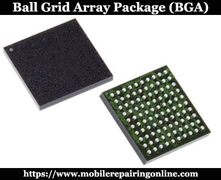
What is a Ball Grid Array (BGA)?
A Ball Grid Array (BGA) is a type of surface-mount packaging used for integrated circuits (ICs). It utilizes a grid of solder balls on the bottom side of the package to provide electrical connections between the IC and the printed circuit board (PCB). BGAs offer several advantages over other packaging types, including high density, excellent electrical and thermal performance, and good reliability.
Key Features of BGAs
- Grid array of solder balls for interconnection
- High pin count and density
- Excellent electrical and thermal characteristics
- Used for complex ICs such as microprocessors, FPGAs, ASICs
BGA Package Construction
A typical BGA package consists of several layers:
1. Substrate – usually made of BT (Bismaleimide Triazine) resin or polyimide, with copper traces for signal routing
2. Solder mask – insulating layer that exposes the solder ball pads
3. Solder balls – lead-free tin-silver-copper (SAC) alloy, typically 0.3-0.6mm in diameter
4. Die – the silicon chip itself, wire-bonded or flip-chip connected to the substrate
5. Encapsulant – epoxy-based material that protects the die
| Layer | Material | Function |
|---|---|---|
| Substrate | BT resin, polyimide | Signal routing |
| Solder mask | Polymer | Insulation, pad exposure |
| Solder balls | Tin-Silver-Copper | Electrical connection |
| Die | Silicon | Integrated circuit |
| Encapsulant | Epoxy | Die protection |
BGA Substrate Types
BGA packages can use different substrate materials depending on the application requirements:
| Substrate | Characteristics | Typical Applications |
|---|---|---|
| BT resin | Low cost, good stiffness | Consumer electronics |
| Polyimide | Higher density, flexible | Mil/aero, medical |
| Ceramic | Best CTE match to die, hermetic | RF, high-reliability |

BGA Advantages
BGAs offer several key benefits compared to other IC package types:
High Density
The grid array configuration allows for a large number of I/O connections in a small package footprint. This is essential for complex, high-performance ICs like processors and FPGAs that require hundreds or even thousands of pins.
Excellent Electrical Performance
With shorter trace lengths and lower inductance than peripheral lead packages, BGAs provide superior electrical characteristics. This enables higher signal speeds and integrity.
Good Thermal Performance
The large number of solder balls and the exposed die pad (if present) provide efficient heat dissipation from the IC to the PCB. This is crucial for high-power devices.
Reliability
When properly designed and assembled, BGAs demonstrate high reliability in various environmental conditions. The underfill material helps redistribute stresses and protects the solder joints.

BGA Design Considerations
Designing with BGAs requires careful attention to several factors:
PCB Layout
- Proper land pattern design is critical for reliable solder joints
- Trace routing should consider signal integrity and avoid crossing split planes
- Thermal relief patterns may be necessary for larger solder balls
Thermal Management
- The PCB should provide adequate heat sinking for high-power BGAs
- Thermal vias and planes can enhance heat transfer
- External heatsinks or fans may be required in some cases
Signal Integrity
- High-speed signals should have controlled impedance traces
- Proper termination and matching are important to minimize reflections
- Ground planes should be used for shielding and current return
Mechanical Stress
- The CTE mismatch between the BGA and PCB can cause stress on the solder joints
- Underfill helps mitigate this stress but requires additional processing
- Stiffeners or support pins may be used for very large BGAs

BGA Assembly Process
The assembly of BGA packages onto PCBs involves several steps:
- Solder Paste Printing
- A stencil is used to apply solder paste to the PCB pads
-
The stencil aperture size and shape must match the solder ball size
-
Component Placement
- The BGA is placed onto the PCB using a pick-and-place machine
-
Precise alignment is critical to ensure proper solder ball contact
-
Reflow Soldering
- The assembly is heated in a reflow oven to melt the solder paste
- The solder balls collapse and form a metallurgical bond with the PCB pads
-
A carefully controlled temperature profile is used to avoid thermal shock
-
Inspection
- X-ray inspection is commonly used to verify solder joint quality
-
Automated optical inspection (AOI) can check for missing or misaligned components
-
Underfilling (optional)
- For enhanced reliability, an epoxy underfill may be applied between the BGA and PCB
- The underfill helps redistribute stresses and protect the solder joints
| Assembly Step | Key Considerations |
|---|---|
| Solder Paste Printing | Stencil aperture design |
| Component Placement | Alignment accuracy |
| Reflow Soldering | Temperature profile |
| Inspection | X-ray, AOI |
| Underfilling | Material selection, dispense process |
BGA Rework and Repair
Despite careful design and assembly, BGAs may sometimes require rework or repair due to manufacturing defects or field failures. The challenges of BGA rework include:
- Localized heating to avoid damaging neighboring components
- Proper removal and replacement of underfill material
- Cleaning and preparing the PCB pads for new component attachment
- Ensuring co-planarity and alignment of the new BGA
Specialized equipment, such as infrared or hot-air rework stations, and skilled operators are necessary for successful BGA rework.
Future Trends in BGA Technology
As IC technology continues to advance, BGA packages are evolving to keep pace:
Finer Pitch
- Smaller solder ball diameters and tighter pitches enable higher density
- Pitches as low as 0.3mm are becoming more common
Advanced Substrates
- Thinner, multilayer substrates with microvias for increased routing density
- Embedded components and 3D packaging technologies for greater functionality
Improved Thermal Solutions
- Integrated heat spreaders and heat pipes for better heat dissipation
- Advanced materials like diamond-filled encapsulants for higher thermal conductivity
Alternative Interconnects
- Copper pillar bumps for finer pitch and better electromigration resistance
- Direct solder ball attachment to the die for lower profile and improved performance
Frequently Asked Questions (FAQ)
1. What is the difference between a BGA and a QFN package?
A BGA has a grid array of solder balls on the bottom side for interconnection, while a QFN (Quad Flat No-lead) has peripheral pads without any leads. BGAs typically have higher pin counts and better thermal performance than QFNs.
2. Can BGAs be soldered using a reflow oven?
Yes, reflow soldering is the standard method for attaching BGAs to PCBs. A controlled temperature profile is used to melt the solder paste and form a reliable bond between the solder balls and PCB pads.
3. What is the purpose of underfill in BGA assembly?
Underfill is an epoxy material that is applied between the BGA and PCB after soldering. It helps redistribute stresses caused by the CTE mismatch between the package and board, protecting the solder joints from fatigue and improving reliability.
4. How can I inspect BGA solder joints for defects?
X-ray inspection is the most common method for evaluating BGA solder joint quality, as the joints are hidden underneath the package. Automated X-ray systems can detect voids, bridges, and other defects. Acoustic micro-imaging is another technique that can reveal cracks and delamination.
5. Are BGAs suitable for high-temperature applications?
BGAs can be designed for high-temperature environments by using appropriate materials and construction techniques. Ceramic substrates, high-Tg underfills, and lead-based solders can extend the temperature range of BGAs. However, careful consideration of the thermal expansion mismatch and stress management is necessary.
Conclusion
Ball Grid Array (BGA) packages have become essential for high-density, high-performance integrated circuits. Their advantages in electrical, thermal, and reliability characteristics make them well-suited for a wide range of applications. However, designing and assembling with BGAs requires careful attention to various factors, from PCB layout to thermal management. As technology advances, BGAs continue to evolve with finer pitches, advanced substrates, and improved thermal solutions. Understanding the fundamentals of BGA technology is crucial for electronics engineers and manufacturers to effectively leverage these packages in their products.


Leave a Reply