What is Back Drilling in PCB Manufacturing?
Back drilling, also known as controlled depth drilling or back-side drilling, is a PCB manufacturing process used to remove unused portions of through-hole vias in high-speed printed circuit board designs. In a standard PCB design, a through-hole via extends through the entire thickness of the board, even if it’s only needed to connect inner layers. The unused portion of the via that extends beyond the last connected layer acts like a stub antenna, causing signal reflections and degrading performance at high frequencies.
Back drilling solves this problem by using a specialized drill to remove the unwanted section of the via from the back side of the board, up to the depth of the last connected layer. This eliminates the stub and improves signal integrity, allowing the PCB to operate at higher frequencies with fewer signal integrity issues.
Benefits of Back Drilling in PCB Design
-
Improved Signal Integrity: By removing the unused portion of the via, back drilling eliminates the stub effect and reduces signal reflections. This leads to cleaner signals and better overall signal integrity, especially at high frequencies.
-
Higher Operating Frequencies: With reduced signal reflections and improved signal integrity, PCBs with back-drilled vias can operate at higher frequencies than those without. This is particularly important for high-speed applications like 5G networks, high-performance computing, and advanced telecommunications systems.
-
Reduced Crosstalk: Back drilling helps minimize crosstalk between adjacent vias by reducing the coupling between them. This is because the removed portion of the via no longer acts as an antenna, picking up and radiating electromagnetic energy.
-
Better Impedance Matching: By removing the stub, back drilling helps maintain consistent impedance throughout the signal path. This is crucial for maintaining signal integrity and preventing reflections caused by impedance mismatches.
-
Increased Reliability: Improved signal integrity and reduced crosstalk lead to more reliable PCB performance overall. This is especially important in critical applications where signal errors could have serious consequences.
The Back Drilling Process
Step 1: PCB Design and Layer Stack-Up
The back drilling process begins with the PCB design itself. The designer must carefully consider the layer stack-up and determine which vias require back drilling. This involves identifying the layers each via needs to connect and calculating the depth to which the via should be drilled.
| Layer | Material | Thickness (mm) |
|---|---|---|
| Top Copper | Copper | 0.035 |
| Prepreg | FR-4 | 0.2 |
| Inner Copper 1 | Copper | 0.018 |
| Core | FR-4 | 0.5 |
| Inner Copper 2 | Copper | 0.018 |
| Prepreg | FR-4 | 0.2 |
| Bottom Copper | Copper | 0.035 |
Example PCB layer stack-up
Step 2: Primary Drilling
Once the PCB design is finalized, the first step in the manufacturing process is primary drilling. This involves drilling all the required through-holes and vias in the board using a standard drill bit. At this stage, the vias extend through the entire thickness of the board.
Step 3: Plating and Etching
After primary drilling, the PCB goes through the standard plating and etching processes to create the copper traces and connect the layers. The through-holes and vias are also plated during this step, creating an electrical connection between the layers.
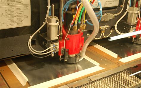
Step 4: Back Drilling
With the PCB fully plated and etched, it’s time for the back drilling process. The board is flipped over, and a specialized drill bit is used to remove the unwanted portion of each designated via from the back side of the board. The depth of the back drill is carefully controlled to ensure it reaches just the right point, typically the last connected layer.
The back drilling process requires high precision to avoid damaging the PCB or the via itself. Modern CNC machines with high-speed spindles and depth control are used to ensure accuracy and consistency.
Step 5: Cleaning and Inspection
After back drilling, the PCB undergoes a thorough cleaning process to remove any debris or residue from the drilling operation. The board is then inspected to ensure all the back-drilled vias are clean, free of burrs, and drilled to the correct depth.

Challenges and Considerations in Back Drilling
While back drilling offers numerous benefits for high-speed PCB designs, it also presents some challenges and considerations for manufacturers and designers alike.
Increased Manufacturing Complexity
Back drilling adds an extra step to the PCB manufacturing process, increasing complexity and production time. It requires specialized equipment and skilled operators to perform the process accurately and consistently. This can impact manufacturing throughput and cost.
Design Considerations
Designers must carefully consider which vias require back drilling and calculate the appropriate drill depths. This requires a deep understanding of the PCB’s layer stack-up and the signal requirements of each via. Inaccurate calculations can lead to insufficient stub removal or, worse, damage to the PCB.
Material Selection
The choice of PCB substrate material can impact the effectiveness of back drilling. Some materials, like high-frequency laminates, may be more brittle and prone to chipping or cracking during the back drilling process. Designers and manufacturers must select materials that can withstand the rigors of back drilling without compromising performance.
Via Positioning
The positioning of vias on the PCB can also affect the feasibility of back drilling. Vias located too close to the edge of the board or to other components may be difficult or impossible to back drill without causing damage. Designers must consider the placement of vias and provide sufficient clearance for the back drilling process.

FAQ
1. Is back drilling necessary for all PCB designs?
No, back drilling is primarily used in high-speed PCB designs where signal integrity is crucial. Lower-frequency designs or those with less stringent signal requirements may not require back drilling.
2. Can back drilling be done manually?
While it’s theoretically possible to perform back drilling manually, it’s not practical or recommended. Back drilling requires high precision and consistency that can only be achieved with CNC machines and specialized drill bits.
3. How much does back drilling add to the cost of PCB manufacturing?
The cost impact of back drilling varies depending on factors like board complexity, the number of vias to be back drilled, and the manufacturing volume. In general, back drilling can add 10-20% to the total PCB manufacturing cost.
4. Can back drilling be used with blind or buried vias?
Yes, back drilling can be used with blind and buried vias, but it requires even greater precision and planning. The depth of the back drill must be carefully calculated to avoid damaging the via or the internal layers of the PCB.
5. Are there any alternatives to back drilling for improving signal integrity?
Other techniques for improving signal integrity in high-speed PCB designs include optimizing via placement, using high-frequency laminates, and employing advanced routing strategies like via stitching or differential pair routing. However, back drilling remains one of the most effective methods for eliminating the stub effect and improving overall signal performance.

Conclusion
Back drilling is a critical technique in modern high-speed PCB manufacturing, enabling designs to operate at higher frequencies with improved signal integrity and reduced crosstalk. By removing the unused portion of through-hole vias, back drilling eliminates the stub effect and provides a cleaner, more consistent signal path.
While back drilling presents some challenges in terms of manufacturing complexity and design considerations, its benefits far outweigh the drawbacks for many high-performance applications. As data rates continue to rise and signal integrity becomes ever more critical, back drilling will likely remain an essential tool in the PCB designer’s and manufacturer’s toolkit.
By understanding the importance of back drilling and the factors that influence its effectiveness, PCB designers and manufacturers can work together to create high-speed, high-reliability PCBs that push the boundaries of performance and functionality.


Leave a Reply