What is AOI Test?
AOI test, or Automated Optical Inspection test, is a non-contact method for inspecting PCBs and other electronic components for defects. The process involves capturing high-resolution images of the product and comparing them to a pre-defined set of design specifications or a “golden sample.” AOI systems use advanced algorithms to detect anomalies, such as missing components, incorrect component placement, solder defects, and circuit pattern errors.
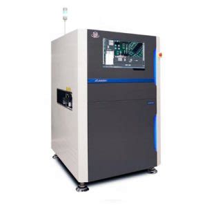
Key Components of an AOI System
An AOI system typically consists of the following components:
- High-resolution cameras
- Lighting system
- Image processing software
- Conveyor or transport mechanism
- User interface and control software
How Does AOI Work?
The AOI testing process can be broken down into the following steps:
-
Image Acquisition: The AOI system captures high-resolution images of the PCB or electronic component from various angles using specialized cameras.
-
Image Processing: The captured images are processed using advanced algorithms to enhance contrast, remove noise, and isolate specific features for analysis.
-
Defect Detection: The processed images are compared to the pre-defined design specifications or golden sample. Any deviations or anomalies are flagged as potential defects.
-
Classification and Reporting: The detected defects are classified based on their type and severity. A report is generated, detailing the location and nature of each defect.
-
Operator Review: In some cases, a human operator may review the defects flagged by the AOI system to confirm their validity and make decisions regarding rework or repair.
Advantages of AOI Testing
Implementing AOI testing in your manufacturing process offers several key benefits:
-
Improved Quality: AOI systems can detect a wide range of defects, ensuring that only high-quality products reach the end customer.
-
Increased Efficiency: Automated inspection is much faster than manual inspection, enabling higher throughput and reduced production time.
-
Cost Reduction: By catching defects early in the manufacturing process, AOI helps reduce scrap, rework, and warranty costs.
-
Consistency: AOI systems provide consistent and objective inspection results, eliminating the variability associated with manual inspection.
-
Traceability: AOI test results can be stored and tracked, providing valuable data for process improvement and quality management.

Applications of AOI Testing
AOI testing is widely used in various industries for inspecting PCBs and electronic components. Some common applications include:
-
PCB Assembly: AOI is used to inspect PCBs after the solder paste printing, component placement, and soldering processes to ensure proper assembly and identify defects.
-
Surface Mount Technology (SMT): AOI is crucial for inspecting SMT components, such as chips, resistors, and capacitors, to verify their presence, placement, and orientation.
-
Through-Hole Technology (THT): AOI can inspect THT components for proper insertion, solder joint quality, and lead placement.
-
Solder Joint Inspection: AOI systems can detect solder defects, such as bridges, insufficient solder, and poor wetting, ensuring reliable electrical connections.
-
Conformal Coating Inspection: AOI can verify the presence and uniformity of conformal coating on PCBs, which is essential for protection against environmental factors.

Best Practices for Implementing AOI Testing
To maximize the benefits of AOI testing, consider the following best practices:
-
Define Clear Inspection Criteria: Establish well-defined acceptance criteria for your products, including dimensional tolerances, component placement, and solder joint quality.
-
Develop a Comprehensive Defect Library: Create a library of known defects and their characteristics to help train your AOI system and improve its defect detection capabilities.
-
Optimize Lighting and Camera Settings: Ensure that your AOI system has appropriate lighting and camera settings to capture high-quality images and minimize false positives or false negatives.
-
Regular Calibration and Maintenance: Regularly calibrate your AOI system and perform preventive maintenance to ensure consistent performance and accuracy.
-
Integrate with Other Quality Control Methods: Use AOI in conjunction with other quality control methods, such as X-ray inspection or functional testing, to provide a comprehensive quality assurance solution.

AOI Test vs. Other Inspection Methods
AOI testing is one of several inspection methods used in electronics manufacturing. Here’s a comparison of AOI with other common inspection techniques:
| Inspection Method | Advantages | Disadvantages |
|---|---|---|
| AOI | Fast, non-contact, detects a wide range of defects | Limited to visible defects, may require additional verification |
| X-ray Inspection | Can detect hidden defects, such as voids or poor solder joints | More expensive, slower than AOI, potential health hazards |
| Manual Inspection | Flexible, can identify complex or unusual defects | Slow, subjective, prone to human error and fatigue |
| Functional Testing | Verifies the electrical performance of the product | Cannot detect visual defects, requires test fixtures and programming |
FAQ
-
What types of defects can AOI test detect?
AOI test can detect a wide range of defects, including missing components, incorrect component placement, solder defects (bridges, insufficient solder, etc.), and circuit pattern errors. -
How does AOI compare to manual inspection in terms of speed and accuracy?
AOI is significantly faster than manual inspection, capable of inspecting hundreds or even thousands of components per minute. Additionally, AOI provides consistent and objective results, reducing the risk of human error and subjectivity associated with manual inspection. -
Can AOI test inspect both sides of a PCB?
Yes, most modern AOI systems are capable of inspecting both sides of a PCB. This is typically achieved by using multiple cameras or a system that can flip the board during the inspection process. -
How do I choose the right AOI system for my manufacturing process?
When selecting an AOI system, consider factors such as the types of defects you need to detect, the size and complexity of your PCBs, the required throughput, and your budget. It’s also important to evaluate the system’s ease of use, scalability, and compatibility with your existing manufacturing equipment and processes. -
What are the limitations of AOI testing?
AOI testing is limited to detecting visible defects on the surface of the product. It cannot detect hidden defects, such as internal voids or poor solder joints beneath components. Additionally, AOI may struggle with inspecting highly reflective or transparent surfaces, and it may require additional verification for complex or unusual defects.
Conclusion
Automated Optical Inspection (AOI) test is a powerful tool for ensuring the quality and reliability of PCBs and electronic components. By automating the inspection process, AOI systems can quickly and accurately detect a wide range of defects, improving efficiency, reducing costs, and ultimately leading to higher customer satisfaction. When implementing AOI testing in your manufacturing process, it’s essential to establish clear inspection criteria, develop a comprehensive defect library, and regularly calibrate and maintain your AOI system. By following best practices and leveraging the advantages of AOI testing, manufacturers can significantly enhance their quality control processes and stay competitive in today’s demanding electronics industry.


Leave a Reply