An Overview of Flexible PCB Technology and Its Applications
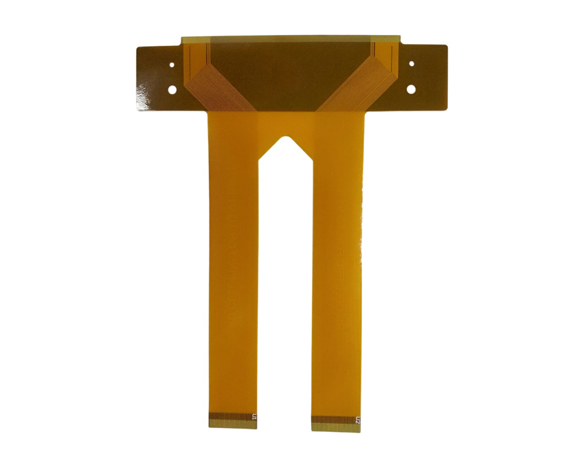
Flexible printed circuit boards (PCBs), also known as flex circuits or flex PCBs, represent an exciting and rapidly growing segment of the PCB fabrication industry. As the name implies, flex PCBs utilize a flexible base material such as polyimide or polyester rather than the traditional rigid fiberglass used in most PCBs. This gives flexible PCBs the ability to bend and flex during use, allowing them to assume dynamic three-dimensional configurations.
Flexible PCBs provide many advantages over their rigid counterparts:
- Weight and space savings from elimination of wiring harnesses
- Dynamic flexing to enable motion or conformal adhesion to surfaces
- Improved reliability with fewer interconnects
- Design freedom through bendable circuits
These benefits make flexible PCBs ideal for many applications:
- Consumer electronics – Cell phones, tablets, cameras
- Automotive – Instrument panels, engine controls, sensors
- Medical – Hearing aids, imaging equipment
- Industrial – Robotics, aviation and aerospace
As flexible PCB technology continues advancing, additional markets are embracing flex circuits for their reliable performance and design flexibility.
Key Design Considerations for Flex PCBs
While flexible PCBs provide exciting design options not possible with rigid boards, they also introduce new considerations to accommodate their dynamic nature:
Flexible Materials
The flexible base material, usually a polyimide or polyester film, requires special handling and process considerations. Most manufacturers limit the minimum bend radius to at least four times the total thickness to avoid damage.
Layer Stackup
Flexible PCB stackups are typically limited to 2-4 conductive layers to minimize thickness and maintain flexibility. Thicker dielectrics are often used to provide adequate insulation between layers.
Dynamic Flexing
Conductors on the flexing portions of the PCB must be arranged perpendicular to the bend axis to avoid fracturing during dynamic flexing motions.
Creepage and Clearance
Larger gaps between conductors may be required for creepage (surface leakage) and clearance (air gap distance) to prevent shorts. Environmental factors such as high humidity impact flex PCB designs.
Stiffeners and Winding Restraints
Rigid stiffeners, frames, and winding restraints are often incorporated to control flexible regions and serve as interfaces or mounting provisions.
Connectors and Components
Connectors, components, and even solder joints need to accommodate flexing movements without compromising connections or performance.
Designing Flexible PCBs with Altium Designer
Altium Designer provides all the tools needed to efficiently design flexible PCBs and harness their advantages. Here are some of the key features:
Flexible Board Outline with Bending Constraints
The board outline can include both rigid and flex regions, along with minimum bend radius constraints to guide layout.
Layer Stack Manager
The layer stack manager allows you to completely customize your layer materials and properties to match your flex PCB manufacturer’s capabilities and recommendations. Flex-specific materials like polyimide and polyester films can be specified.
Dynamic Flexing Analysis
The DFA analyzer highlights conductive traces perpendicular to flex contours that are at risk of fracturing during bending. The layout can then be adjusted to ensure conductors reliably withstand dynamic flexing.
Flexible Region Splitting
Long flexible regions can be split into smaller sections using rigid-flex splitting vias to provide precise control over flexing movements. Stiffener locations are also defined.
3D PCB Modeling
Altium Designer allows you to interactively bend and shape flexible PCB models in 3D space to validate the design intent. Collision detection ensures sufficient clearances.
These advanced capabilities make Altium Designer the premier solution for designing, analyzing, and modeling innovative flexible PCBs to meet demanding application requirements.
A Flex PCB Design Process Overview
While the exact flexible PCB design process can vary between organizations and product requirements, some typical high-level steps include:
- Define rigid and flex regions in the board outline
- Plan layer stackup, materials, and properties
- Floorplan components and routing, mindful of flex clearances
- Run DFA analysis on dynamic regions
- Incorporate stiffeners, frames, and winding restraints
- Review clearances, creepage, manufacturability
- Create/integrate 3D flexing models
- Validate design rules and electrical analysis
- Export design files and fabricate prototypes
- Assemble, test, inspect, and refine if needed
- Finalize design and move to mass production
Careful planning is needed upfront to accommodate flex PCB constraints, but the benefits are worth the extra design considerations.
Applications and Examples of Flexible PCBs
To illustrate the versatility of flexible PCBs, here are some examples across different products and industries:
Consumer Electronics
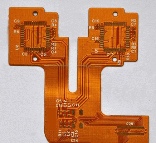
Flexible PCBs are ubiquitous in consumer electronics like mobile phones and wearables. A flex can connect the main rigid PCB to displays, cameras, or other modules as devices become more packed and complex. Dynamic flexing accommodates sliding and folding motions.
Automotive
Inside cars, flex PCBs mount on complex 3D surfaces like dashboards and center consoles to control electronics. Flexible connections between steering wheel buttons, sensors, and displays enable modular assemblies.
Medical Equipment
Medical devices like hearing aids often require flexible PCBs to conform to the body or fit into ergonomic cases. Flex circuits also connect sensors used in advanced imaging and diagnostic equipment.
Industrial
In robots and automation systems, flex PCBs accommodate moving joints and mechanisms between rigid PCB assemblies. Their dynamic bend radius allows smooth and reliable motion.
Aerospace and Aviation
Aerospace applications use flex PCBs to save weight and wiring. The boards can be produced with high-reliability materials to withstand temperature extremes and vibration while connecting flight control systems.
As these examples demonstrate, flexible PCB technology enables innovative solutions across many industries and use cases where dynamic movement, flexing, or 3D conformal fit are required.
Common Questions About Flexible PCBs
Here are answers to some frequently asked questions about flexible PCB design and manufacturing:
What are the typical layers used in flex PCBs?
Flex PCBs typically use a single, double, or multilayer stackup with 2 to 6 conductive layers. Common flexible materials are polyimide and polyester films in thicknesses from 1 mil up to about 5 mils. Adhesives join the film layers.
Can components be mounted directly on flex PCBs?
Yes, but the flexing nature requires use of special flexible packages or connectors. Rigid islands with stiffeners are often used for mounting heavier components. Careful mechanical stress analysis helps determine suitable components.
What are recommended minimum dimensions for flex PCB conductors?
As a general rule, 6 mil minimum trace/space is recommended for outer layers and 8 mil for inner layers. High layer counts may require thicker traces. These minimums ensure conductivity and manufacturability.
What design rules guide rigid-to-flex transitions?
Smooth transitions with maximum slopes of 45-90 degrees avoid failures. Non-flex layers should not extend beyond flexible layers by more than 0.15mm to avoid peaks in bending stress.
How are vias constructed in multilayer flex PCBs?
Stacked and staggered microvias with 6-12mil diameters are used to connect layers rather than through-hole or buried vias. Careful registration helps ensure reliable interlayer connections.
Conclusion
Flexible PCBs provide many advantages that continue driving increased adoption across diverse applications, from consumer gadgets to mission-critical systems. Altium Designer offers advanced tools to help designers harness the benefits of flex circuits while navigating their unique constraints and complexity. By following sound design practices and leveraging technology like DFA analysis and 3D modeling, innovative flexible PCBs can be designed efficiently, simulated digitally, and manufactured successfully. The future looks bright and flexible as this technology evolves and enables the next generation of electronics.


Leave a Reply