Introduction to the AD9850 DDS Module
The AD9850 is a highly integrated device that uses advanced DDS technology coupled with an internal high speed, high performance D/A converter and comparator to form a complete digitally programmable frequency synthesizer and clock generator function. It is capable of generating frequencies from 1 Hz to 62.5 MHz with 32-bit frequency resolution.
Key features of the AD9850 include:
- 125 MHz internal clock speed
- 32-bit frequency tuning word
- 5 V single supply operation
- Serial loading interface
- Analog and digital output modes
- Excellent temperature stability
The AD9850 DDS module is a popular, low-cost board that provides an easy way to experiment with the AD9850 chip and generate precision frequencies for various applications such as:
- RF signal generation
- Frequency sweeping and modulation
- Programmable clock generation
- Arbitrary waveform synthesis
- Digital radio and software-defined radio (SDR)
AD9850 Module Specifications
| Parameter | Value |
|---|---|
| Frequency Range | 0 to 62.5 MHz |
| Frequency Resolution | 32-bit (0.0291 Hz at 125 MHz clock) |
| Output Waveform | Sine, Triangle, Square |
| Output Amplitude | 0 to 1 Vpp (typical) |
| Supply Voltage | 5 V |
| Interface | Serial (W_CLK, FQ_UD, D7, RESET) |
| Board Dimensions | 30 x 20 mm (approx.) |
How the AD9850 Works
The AD9850 generates frequencies using a technique called direct digital synthesis (DDS). DDS works by storing the points of a waveform in digital format and then using a D/A converter to generate the analog output signal.
The core components of the AD9850 include:
-
Phase Accumulator: A 32-bit register that increments by the frequency tuning word (FTW) on each clock cycle. The phase accumulator generates a digital sawtooth waveform.
-
Phase-to-Amplitude Converter: Converts the phase information from the accumulator into a digital amplitude value using a sine lookup table (ROM).
-
D/A Converter: Converts the digital amplitude into an analog signal. The AD9850 uses a 10-bit DAC.
-
Comparator: Generates a square wave output from the DAC signal.
-
Serial Interface: Allows loading the frequency tuning word and control bits via a 40-bit serial data stream.
The frequency tuning word (FTW) determines the output frequency according to the formula:
f_out = (FTW * f_clk) / 2^32
Where:
– f_out is the output frequency
– FTW is the 32-bit frequency tuning word
– f_clk is the AD9850 reference clock frequency (usually 125 MHz)
– 2^32 is 4,294,967,296 (2 to the power of 32)
For example, to generate a 10 MHz output with a 125 MHz clock, the FTW would be:
FTW = (10,000,000 * 2^32) / 125,000,000 = 343,597,383
In hexadecimal, this is 0x147AE147.

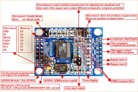
Pinout and Connections
The AD9850 module has the following pinout:
| Pin | Name | Description |
|---|---|---|
| 1 | GND | Ground |
| 2 | VCC | 5 V power supply |
| 3 | W_CLK | Serial clock input |
| 4 | FQ_UD | Frequency update |
| 5 | D7 | Serial data input |
| 6 | RESET | Reset signal |
| 7 | OUT | Analog output |
| 8 | COMP | Comparator output |
To use the AD9850 module, make the following connections:
- Connect VCC to a 5 V power supply and GND to ground.
- Connect W_CLK, FQ_UD, D7, and RESET to the appropriate microcontroller pins for serial communication.
- Connect OUT to an oscilloscope or other equipment to observe the analog output signal.
- (Optional) Connect COMP to view the square wave output.
Connecting to a Microcontroller
To control the AD9850 module, you’ll need to connect it to a microcontroller that supports serial communication. Popular choices include Arduino, Raspberry Pi, and STM32 boards.
Here’s an example wiring diagram for connecting the AD9850 to an Arduino Uno:
AD9850   Arduino
---------------
VCC      5V
GND      GND
W_CLK    D8
FQ_UD    D9
D7       D10
RESET    D11

Serial Communication Protocol
The AD9850 uses a simple serial interface to load the frequency tuning word and control settings. The serial data is clocked in on the rising edge of W_CLK, and the FQ_UD pin is used to latch the data into the AD9850’s internal registers.
The serial data format consists of 40 bits:
| Bits | Description |
|---|---|
| 39-8 | 32-bit frequency tuning word (FTW) |
| 7 | Power-down bit (0 = normal operation, 1 = power-down) |
| 6 | Phase and frequency reset (0 = reset, 1 = normal operation) |
| 5 | Sleep reset (0 = reset, 1 = normal operation) |
| 4 | Reserved (set to 0) |
| 3 | Not used |
| 2 | Not used |
| 1-0 | Control bits for COMP output |
To load data into the AD9850:
- Set FQ_UD low.
- Clock in the 40-bit serial data, MSB first, on the rising edge of W_CLK.
- Set FQ_UD high to latch the data into the AD9850’s registers.
Here’s an example timing diagram:
          _   _   _   _   _   _   _   _   _   _   _   _   _   _   _   _
W_CLK   _| |_| |_| |_| |_| |_| |_| |_| |_| |_| |_| |_| |_| |_| |_| |_| |
          ___________________________________________________________
FQ_UD   _|                                                           |____
          ___________________________________________________________
D7      _|_D39__|_D38_|_..............................................|_D0_

Programming the AD9850
To generate a specific frequency with the AD9850, you’ll need to calculate the frequency tuning word (FTW) and send it to the module using the serial interface.
Here’s a step-by-step guide:
- Calculate the FTW using the formula:
FTW = (desired_freq * 2^32) / ref_clock_freq. - Convert the FTW to a 32-bit binary number.
- Add the control bits to form the complete 40-bit serial data.
- Send the serial data to the AD9850 using the timing sequence described in the previous section.
Here’s an example Arduino sketch that generates a 10 MHz signal:
#define W_CLK 8
#define FQ_UD 9
#define DATA 10
#define RESET 11

const long refClockFreq = 125000000;
const long freq = 10000000;

void setup() {
  pinMode(W_CLK, OUTPUT);
  pinMode(FQ_UD, OUTPUT);
  pinMode(DATA, OUTPUT);
  pinMode(RESET, OUTPUT);

  digitalWrite(RESET, LOW);
  digitalWrite(RESET, HIGH);

  setFrequency(freq);
}

void loop() {
  // Your code here
}

void setFrequency(long frequency) {
  long ftw = (frequency << 32) / refClockFreq;

  digitalWrite(FQ_UD, LOW);

  for (int b = 31; b >= 0; b--) {
    digitalWrite(DATA, (ftw >> b) & 1);
    digitalWrite(W_CLK, HIGH);
    digitalWrite(W_CLK, LOW);
  }

  // Control bits all 0 for simplicity
  for (int i = 0; i < 8; i++) {
    digitalWrite(DATA, LOW);
    digitalWrite(W_CLK, HIGH);
    digitalWrite(W_CLK, LOW);
  }

  digitalWrite(FQ_UD, HIGH);
}
Applications and Examples
The AD9850 module can be used in a wide range of applications that require precise frequency generation or synthesis. Here are a few examples:
RF Signal Generator
Build a simple RF signal generator by connecting the AD9850’s output to an amplifier and low-pass filter. Use a microcontroller to set the frequency and provide a user interface (e.g., LCD, buttons).
Sweep Generator
Create a frequency sweep generator by continuously updating the AD9850’s frequency tuning word. This can be useful for testing filters, characterizing resonant circuits, or measuring frequency response.
Digital Radio Transmitter
Use the AD9850 as a local oscillator in a digital radio transmitter. Modulate the signal using amplitude modulation (AM), frequency modulation (FM), or phase modulation (PM) techniques.
Clock Generator
Generate custom clock signals for digital circuits, microcontrollers, or FPGAs. The AD9850’s high-resolution frequency control allows for fine-tuning of the clock frequency.
Troubleshooting and Tips
- Make sure the AD9850 module is powered with a clean, stable 5 V supply. Noise or fluctuations can affect the output signal quality.
- Use decoupling capacitors (e.g., 0.1 uF) close to the VCC pin to reduce high-frequency noise.
- Keep the wiring between the AD9850 and microcontroller short to minimize interference and signal degradation.
- If the output signal has distortion or spurious frequencies, try adding a low-pass filter to the output.
- Be aware of the AD9850’s output impedance (approx. 50 ohms) when connecting it to other circuits or loads.
- Use shielded cables for the output signal to reduce electromagnetic interference (EMI).
FAQ
Q1: What is the maximum frequency the AD9850 can generate?
A1: The AD9850 can generate frequencies up to 62.5 MHz, which is half of its 125 MHz reference clock frequency.
Q2: How do I change the output frequency of the AD9850?
A2: To change the output frequency, calculate the new frequency tuning word (FTW) and send it to the AD9850 via the serial interface. The FTW determines the output frequency based on the reference clock frequency.
Q3: Can I use a different reference clock frequency?
A3: Yes, you can use a different reference clock frequency by providing an external clock signal to the AD9850. However, keep in mind that this will change the frequency resolution and maximum output frequency.
Q4: What is the frequency resolution of the AD9850?
A4: The frequency resolution depends on the reference clock frequency and the 32-bit frequency tuning word. With a 125 MHz clock, the resolution is 0.0291 Hz (125 MHz / 2^32).
Q5: How do I connect the AD9850 to a microcontroller?
A5: Connect the AD9850’s serial interface pins (W_CLK, FQ_UD, D7, RESET) to the appropriate pins on your microcontroller. Typically, you’ll use digital output pins and follow the serial communication protocol described in the datasheet.
Conclusion
The AD9850 DDS module is a versatile and low-cost solution for generating precise frequencies in a wide range of applications. By understanding the principles of direct digital synthesis, the AD9850’s serial interface, and the frequency tuning word calculation, you can easily integrate this module into your projects and experiments.
Remember to follow best practices for wiring, power supply, and signal integrity to ensure optimal performance. With the AD9850, you can explore the world of frequency synthesis, RF engineering, and digital signal processing. Happy experimenting!


Leave a Reply