Understanding the Basics of PCB Manufacturing
Before we explore the PCB manufacturing process in detail, let’s start with some fundamental concepts and terminology.
What is a PCB?
A Printed Circuit Board (PCB) is a flat, thin board made of insulating materials, such as fiberglass or composite epoxy, with conductive pathways printed or etched onto its surface. These pathways, known as traces or tracks, connect various electronic components, such as resistors, capacitors, and integrated circuits (ICs), to form a functional electronic circuit.
Types of PCBs
PCBs can be classified based on the number of layers and the density of components:
- Single-sided PCBs: These have conductive traces on only one side of the board.
- Double-sided PCBs: These have conductive traces on both sides of the board, with through-hole connections called vias.
- Multi-layer PCBs: These consist of three or more conductive layers separated by insulating layers, allowing for more complex circuits and higher component density.
PCB Design Software
PCB design software tools are used to create the schematic and layout of the PCB. Some popular PCB design software include:
- Altium Designer
- OrCAD
- Eagle
- KiCad
These tools help engineers and designers create accurate and optimized PCB designs, ensuring proper component placement, trace routing, and adherence to manufacturing constraints.
The PCB Manufacturing Process
The PCB manufacturing process can be divided into several key stages:
- PCB Design and Verification
- PCB Fabrication
- PCB Assembly
- Testing and Quality Control
Let’s explore each of these stages in detail.
1. PCB Design and Verification
The first step in the PCB manufacturing process is to design the PCB using specialized software tools. This involves creating a schematic diagram that represents the electrical connections between components and then translating this schematic into a physical layout.
Schematic Design
The schematic design is a graphical representation of the electronic circuit, showing the components and their interconnections using standardized symbols. The schematic captures the logical connections between components without considering their physical placement on the PCB.
PCB Layout Design
Once the schematic is complete, the next step is to create the PCB layout. This involves arranging the components on the board and routing the traces to connect them according to the schematic. The layout design must consider various factors, such as:
- Component placement for optimal signal integrity and thermal management
- Trace width and spacing to minimize signal interference and ensure manufacturability
- Via placement and drilling requirements
- Manufacturing constraints, such as minimum feature sizes and clearances
Design Rule Check (DRC) and Verification
After completing the PCB layout, it is essential to perform a Design Rule Check (DRC) to ensure that the design meets all the manufacturing constraints and guidelines. DRC software tools analyze the layout for potential issues, such as insufficient clearances, trace width violations, or missing connections.
Additionally, the design may undergo simulation and verification to assess its electrical performance, signal integrity, and electromagnetic compatibility (EMC). This helps identify and rectify any potential issues before proceeding to fabrication.
2. PCB Fabrication
Once the PCB design is finalized and verified, the fabrication process begins. PCB fabrication involves several steps that transform the raw materials into a functional printed circuit board.
Material Preparation
The first step in PCB fabrication is to prepare the raw materials. The most common base material for PCBs is FR-4, a type of fiberglass-reinforced epoxy laminate. Other materials, such as polyimide or high-frequency laminates, may be used for specific applications.
The base material is cut to the required size and thickness, and a layer of copper foil is laminated onto one or both sides of the board using heat and pressure.
Drilling
After the copper-clad laminate is prepared, the next step is to drill holes for through-hole components and vias. The drilling process is typically done using computer numerical control (CNC) machines that follow the drill file generated from the PCB design software.
Patterning
The patterning process is used to create the conductive traces on the PCB surface. There are two primary methods for patterning: subtractive and additive.
- Subtractive patterning:
- The entire copper surface is coated with a photoresist material.
- The photoresist is exposed to UV light through a photomask that contains the trace pattern.
- The exposed photoresist is developed, leaving the desired trace pattern protected.
- The unprotected copper is etched away using a chemical solution, typically ferric chloride or ammonium persulfate.
-
The remaining photoresist is removed, revealing the copper traces.
-
Additive patterning:
- A thin layer of photoresist is applied to the bare substrate.
- The photoresist is exposed to UV light through a photomask with the inverse of the trace pattern.
- The exposed photoresist is developed, leaving the desired trace pattern exposed.
- Copper is electroplated onto the exposed areas, forming the traces.
- The remaining photoresist is removed, leaving only the copper traces on the substrate.
Lamination and Multilayer Fabrication
For multi-layer PCBs, the fabrication process involves additional steps to stack and laminate the individual layers together.
- Each layer is patterned using the subtractive or additive method described above.
- The layers are aligned and stacked together with insulating prepreg (pre-impregnated) sheets between them.
- The stack is placed in a press and subjected to heat and pressure to bond the layers together.
- Holes are drilled through the laminated board to create vias that connect the layers electrically.
- The holes are plated with copper to ensure proper electrical connection between layers.
Surface Finishing
After the patterning and lamination processes, the PCB undergoes a surface finishing process to protect the exposed copper and improve solderability. Common surface finishes include:
- Hot Air Solder Leveling (HASL): The PCB is dipped in molten solder and then leveled using hot air knives.
- Organic Solderability Preservative (OSP): A thin, organic coating is applied to the copper surface to prevent oxidation.
- Electroless Nickel Immersion Gold (ENIG): A layer of nickel is deposited on the copper, followed by a thin layer of gold.
- Immersion Silver: A thin layer of silver is deposited on the copper surface.
Solder Mask Application
A solder mask is a protective coating applied to the PCB surface, leaving only the areas intended for soldering exposed. The solder mask helps prevent solder bridges and short circuits during the assembly process.
The solder mask is typically applied using a screen printing or photoimaging process, and then cured using UV light or heat.
Silkscreen
The final step in PCB fabrication is the application of the silkscreen. The silkscreen is a layer of text and symbols printed on the PCB surface to aid in component placement and identification during assembly. The silkscreen is typically printed using a screen printing process and then cured.
3. PCB Assembly
After the fabrication process is complete, the PCB is ready for assembly. PCB assembly involves placing and soldering components onto the board according to the design specifications.
Component Placement
Components are placed on the PCB using automated pick-and-place machines or manually, depending on the complexity and volume of the production run. The placement machine reads the component locations from the PCB design files and places the components accurately on the board.
Soldering
After the components are placed, the PCB undergoes a soldering process to create electrical connections between the components and the traces. There are two primary soldering methods:
- Wave Soldering: The PCB is passed over a molten solder wave, which solders the through-hole components to the board.
- Reflow Soldering: A solder paste, containing tiny solder particles suspended in flux, is applied to the PCB pads using a stencil or screen printing process. Surface mount components are then placed on the solder paste. The board is passed through a reflow oven, which melts the solder particles and creates a permanent connection between the components and the pads.
4. Testing and Quality Control
After the PCB assembly is complete, the board undergoes various testing and quality control procedures to ensure its functionality and reliability.
Visual Inspection
The first step in quality control is a visual inspection of the assembled PCB. This inspection checks for obvious defects, such as missing or misaligned components, solder bridges, or damaged components.
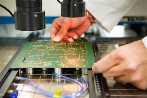
Automated Optical Inspection (AOI)
An AOI machine uses high-resolution cameras and image processing algorithms to inspect the PCB for defects that may be difficult to detect with the naked eye. AOI can identify issues such as incorrect component placement, solder defects, or trace anomalies.
In-Circuit Testing (ICT)
ICT is a testing method that verifies the electrical connectivity and functionality of individual components on the PCB. An ICT fixture, which contains a bed of nails or probes, makes contact with specific test points on the PCB and applies electrical signals to test the components and their connections.
Functional Testing
Functional testing involves powering up the PCB and testing its overall functionality as a complete system. This testing may include running specific test routines or software to verify that the PCB performs as intended.
Boundary Scan Testing
Boundary scan testing, also known as JTAG testing, is a method used to test complex digital circuits, such as those containing high-density ball grid array (BGA) components. This testing method uses a special test access port (TAP) built into the components to access and test their internal circuitry.

Frequently Asked Questions (FAQ)
-
Q: What is the difference between a PCB and a PCBA?
A: A PCB (Printed Circuit Board) is the bare board with copper traces and pads, while a PCBA (Printed Circuit Board Assembly) is a PCB with components soldered onto it, ready for use in an electronic device. -
Q: What are the advantages of using a multi-layer PCB?
A: Multi-layer PCBs offer several advantages, such as increased circuit density, improved signal integrity, better electromagnetic compatibility, and reduced board size. They are ideal for complex electronic devices that require high-performance and compact design. -
Q: What is the purpose of a solder mask on a PCB?
A: A solder mask is a protective coating applied to the PCB surface that prevents solder from bridging between traces and pads during the assembly process. It also provides insulation and protection against environmental factors, such as moisture and dust. -
Q: Why is testing important in the PCB manufacturing process?
A: Testing is crucial to ensure the quality, reliability, and functionality of the manufactured PCB. It helps identify defects and issues that may affect the PCB’s performance or cause failures in the final electronic device. By detecting and addressing these issues early in the manufacturing process, manufacturers can save time and costs associated with rework or product returns. -
Q: What are the key factors to consider when selecting a PCB manufacturer?
A: When choosing a PCB manufacturer, consider factors such as their experience and expertise in the specific type of PCB you require, their manufacturing capabilities and capacity, their quality control and testing procedures, their turnaround time and pricing, and their customer support and communication. It is also essential to ensure that the manufacturer adheres to industry standards and certifications, such as ISO 9001, IPC, or UL, depending on your requirements.

Conclusion
The PCB manufacturing process is a complex and multi-stage endeavor that requires precision, expertise, and adherence to strict quality standards. From design and fabrication to assembly and testing, each step plays a crucial role in determining the final quality and functionality of the PCB.
By understanding the various stages and techniques involved in PCB manufacturing, engineers, designers, and manufacturers can work together to create high-quality, reliable, and cost-effective PCBs that power the electronic devices we rely on every day.
As technology continues to advance and the demand for more complex and compact electronic devices grows, the PCB manufacturing industry will need to adapt and innovate to meet these challenges. This may involve the development of new materials, processes, and testing methods to ensure that PCBs can keep pace with the ever-evolving world of electronics.


Leave a Reply