Introduction
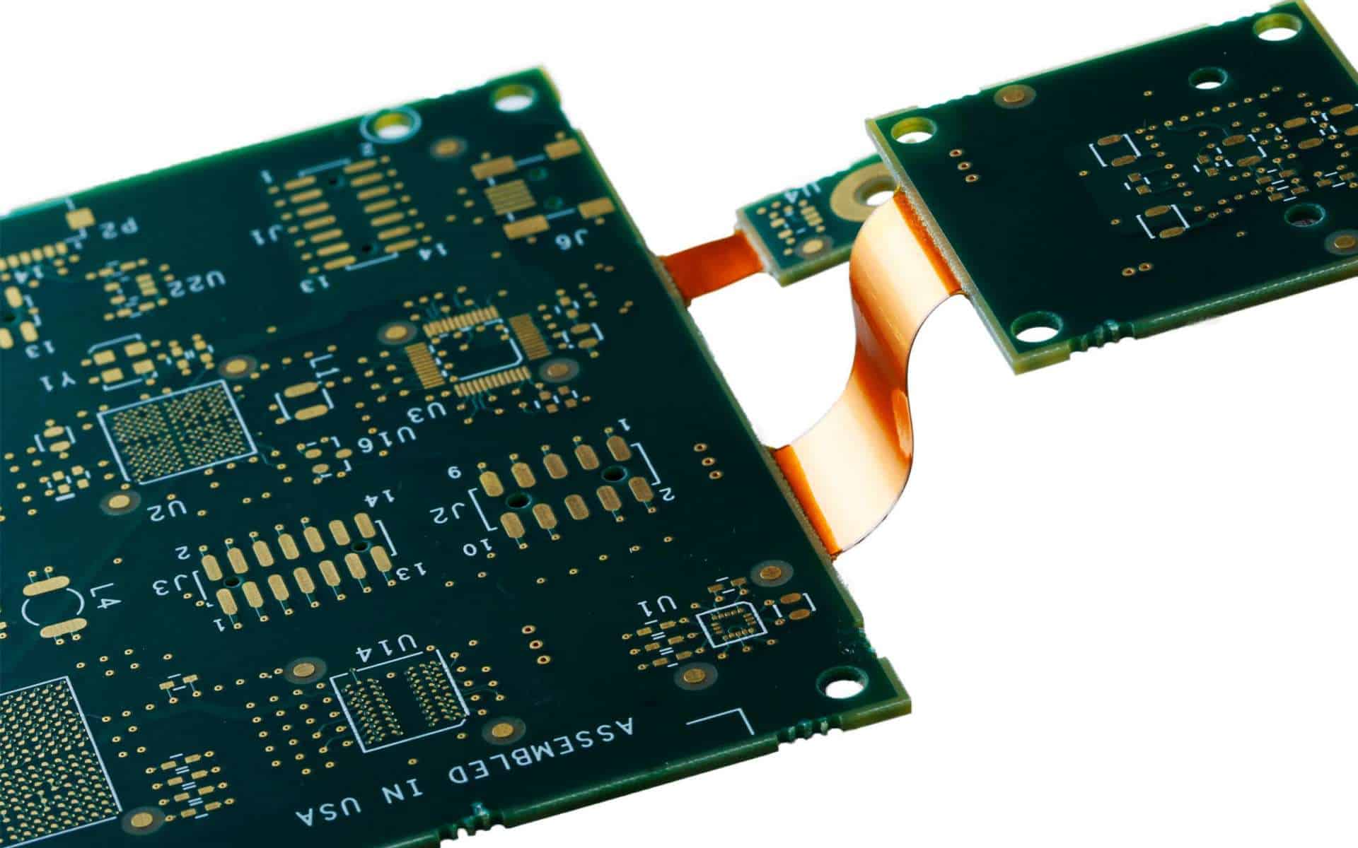
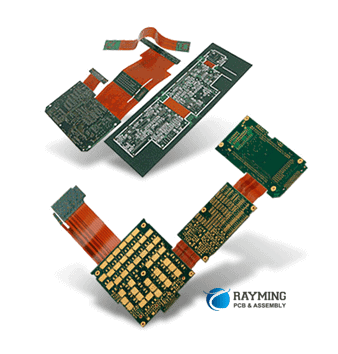
Rigid-flex printed circuit boards (PCBs) combine rigid and flexible circuitry into a single integrated assembly. They provide solutions for applications where flexible and dynamic interconnections are required between multiple rigid PCBs. Rigid-flex PCBs allow three-dimensional wiring to interconnect rigid PCBs and components. This enables more efficient use of space compared to traditional cabling or connectors between rigid PCBs.
Rigid flex PCB stackup refers to the sequence of material layers that make up the rigid-flex board. Proper stackup design is critical for reliable performance of rigid-flex PCBs. The stackup must balance electrical, mechanical, and manufacturing requirements. This article provides an overview of rigid flex PCB stackup design considerations.
Rigid Layer Stackup
The rigid portions of a rigid-flex PCB typically have a conventional rigid PCB layer stackup. This includes:
- Copper layers for traces and pads
- Dielectric layers for insulation between copper
- Prepreg bonding layers
- Stiffeners to control thickness and stiffness
The number of conductive copper layers and dielectric layers can be varied according to circuit complexity and layer count needs. Common rigid layer counts are 4, 6, 8, and more recently 10-12+ layers.
The stackup sequence and materials must be engineered to provide the required stiffness, thermal management, and electrical performance. The thickness of each rigid section must also be controlled. Standard PCB laminates like FR-4 are commonly used. More advanced materials can be used when higher performance is needed.
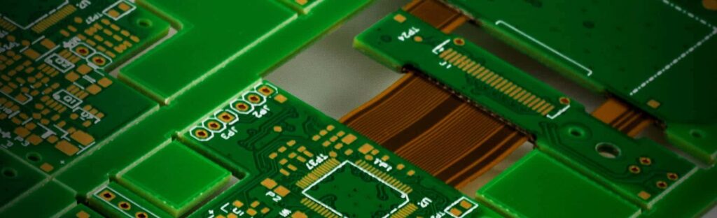
Flex Layer Stackup
The flexible sections of the rigid-flex PCB must be designed for dynamic bending and flexing. A typical flex stackup contains:
- Flexible copper conductors
- Flexible dielectric like polyimide
- Cover layers or solder mask for insulation
The flexible layers are typically very thin – around 25-100 microns per layer. This allows tight bending radii of 3mm or less. Two to four conductive layers are typical for most flex applications. The conductors are often annealed copper foils that can withstand repeated bending stress. Polyimide films like Kapton are widely used as the flexible dielectric.
Controlling the overall thickness and layer symmetry is critical in the flex stackup. Unbalanced stackups can lead to curling or twisting of the flex layers. Balanced configurations with cover layers on both sides are often preferred.
Bonded Rigid-Flex Stackup
Creating the complete rigid-flex PCB stackup requires bonding the rigid and flex layers together into an integrated assembly. There are two main approaches:
1. Sequential Bonding
In this method, the rigid and flex layers are fabricated separately. The flex circuitry is etched first. The pre-etched flex layers are then bonded to the rigid board during lamination. This allows maximum flexibility in the rigid and flex layer counts and materials. It also reduces stresses from coefficient of thermal expansion (CTE) mismatches between the sections. However, it requires precision alignment during bonding and can limit routing density across the rigid-flex interface.
2. Monolithic Fabrication
With this technique, the rigid and flex layers are stacked up together and then fabricated as a single PCB. This allows seamless transitions between the rigid and flex areas. It enables higher interconnect density across the interface. The disadvantage is that CTE mismatches can induce stresses and distortions. The fabrication process must also accommodate the different requirements of rigid and flex materials in the same board.
Stackup Design Guidelines
To create a successful rigid-flex PCB stackup, engineers should follow these guidelines:
- Balance layer thicknesses – Symmetrical stackups minimize curling or warpage
- Manage CTE mismatches – Use low/ultra-low expansion materials to reduce stresses
- Model bending stresses – Verify stackup can handle required dynamic flexing
- Allow for thick components – Ensure adequate clearance in rigid sections
- Control impedance – Stackup affects signal quality in high-speed design
- Validate manufacturability – Work with fabricators to confirm process capability
Prototyping and design validation are critical to catch any issues before full production.
Applications and Examples
Rigid-flex PCBs enable unique solutions across many industries:
Aerospace and Defense
Rigid-flex can package circuits into cramped missiles and satellites. Stackups are engineered for extreme environments. Flexible sections allow dynamic connections and mechanisms.
Medical
Thin, wearable devices benefit from integrated rigid and flex circuits. Tight stackups are needed to fit into compact devices. Flexibility allows bending around organs.
Consumer Electronics
Foldable smartphones, laptops, and displays take advantage of flexible circuits. Dynamic bending requires extremely thin and robust flex stackups.
Automotive
Interconnects for cameras, sensors, and displays use rigid-flex configurations. Vibration resistance and reliability are key requirements.
Rigid-Flex PCB Stackup Design Process
Here is a general process for designing the stackup on a complex rigid-flex PCB:
- Define circuit requirements – Determine layer count, high-speed signals, component clearance, etc.
- Select rigid materials – Choose base PCB laminates suitable for layer count, frequency, etc. Consider thermal and mechanical needs.
- Choose flexible materials – Thin polyimide films able to meet bending requirements. Ensure IPC compatibility.
- Create initial stackup – Sketch layer sequence, paste masks, cross-sections. Include any special materials like cover coats.
- Model stackup – Build model in PCB design software and simulate mechanical, thermal, and electrical performance.
- Analyze results – Look for issues like excessive stress, impedance mismatches, resonances.
- Refine stackup – Iterate on layer sequence, thicknesses, and materials. Redo models and analysis.
- Finalize design – Complete detailed stackup drawing for fabrication. Specify materials, finishes, and tolerances.
- Prototype – Build samples and test for functionality, reliability under bending, EMI, etc.
- Qualify – Put through applicable qualification testing to validate robustness.
Rigid-flex stackups require extensive modeling, analysis and verification to ensure reliable functionality in the application. Close coordination with an experienced rigid-flex PCB manufacturer is highly recommended.
FQA
What are some key considerations for rigid-flex PCB stackup design?
Some key considerations include:
- Balancing layer thicknesses and materials between rigid and flex areas
- Minimizing mechanical stresses from CTE mismatches
- Controlling stackup thickness, especially in flex areas
- Managing impedance for high-speed signals
- Allowing for clearance of rigid-mounted components
- Validating manufacturability and reliability
What are some typical flexible dielectric materials used?
Common flexible dielectric materials include polyimide films like Kapton, Apical, Ube, and DuPont Pyralux. Flexible LCP films are also sometimes used. Thicknesses range from around 12 microns to 125 microns.
How many conductive layers are typical in the rigid vs. flex sections?
The rigid sections often have higher layer counts of 8 layers or more to accommodate complex circuitry. The flexible sections typically have 1-4 conductive layers since the thin stackup limits layer count.
What are some ways to manage differences in CTE between rigid and flex areas?
Using low or ultra-low CTE laminates like PPO or LCP in the rigid sections helps minimize CTE mismatches. Balanced symmetrical stackups on the flex layers also reduces stresses. Strategic placement of the interface region is important. Stress relief features may also be used.
How small can bending radii be with rigid-flex PCBs?
Typical bending radii for rigid-flex PCBs are around 2-5mm. With very thin flex stacks (<60um) even tighter radii below 2mm are possible. The required radius depends on materials, number of layers, and dynamic bending requirements.


Leave a Reply