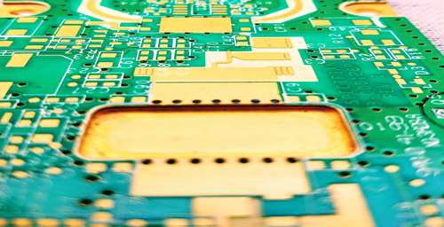
Rigid printed circuit boards (rigid PCBs) are the most common type of printed circuit board (PCB) used in electronics manufacturing. As the name suggests, rigid PCBs have a rigid, non-flexible structure made from materials like FR-4 glass epoxy.
Rigid PCBs provide a sturdy foundation for mounting and interconnecting electronic components using conductive copper traces etched from copper sheets laminated onto a non-conductive substrate. Compared to flexible PCBs, rigid PCBs offer higher circuit density with smaller traces and spaces. They are more rugged and better suited for complex, high-performance circuits.
Key Features of Rigid PCBs
Rigid PCBs have the following key features:
Non-Flexible Substrate
The substrate or base material of rigid PCBs consists of sheets of woven fiberglass cloth impregnated with epoxy resin (FR-4). This composite material is rigid and strong enough to support mounted electronic components. Other substrates like ceramics and synthetics are also used sometimes.
Copper Layer Stackup
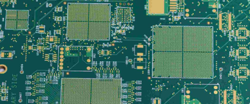
Rigid PCBs have a multi-layer copper stackup consisting of thin copper foil laminated to the substrate. Complex PCBs can have 8-12 copper layers or more. The layers are interconnected with plated-through holes.
High Circuit Density
Small trace widths and spaces down to 2-3 mils are possible with rigid PCB fabrication. This allows packing more circuitry and routing complex interconnections on a small PCB area.
Thermal Stability
The rigid FR-4 substrate offers dimensional stability and withstands heat during PCB assembly soldering processes and component operation. This makes rigid PCBs suitable for high power circuits.
Easy Assembly
The flat shape and rigid structure of PCBs make component mounting and soldering easier with standardized assembly processes. Through-hole and surface mount assembly are easily done on rigid PCBs.
Typical Applications of Rigid PCBs
Here are some typical applications taking advantage of the features of rigid PCBs:
- Consumer electronics – Cellphones, routers, home appliances
- Computers – Motherboards, graphics cards, storage devices
- Automotive electronics – Engine control units, battery management systems
- Industrial equipment – PLCs, process controllers, instrumentation
- Medical devices – Diagnostic equipment, surgical tools
- Aerospace avionics – Flight management systems, engine controls
In short, rigid PCBs are used in nearly every electronics product that requires a robust circuit foundation. The demand for PCBs continuously grows as technology advances and new applications emerge.
Rigid PCB Materials and Construction
Rigid PCB construction aims to create a sturdy multi-layer board with complex copper interconnections. Here are the key materials and construction methods used.
Substrate Materials
The substrate forms the core layer of the PCB providing mechanical support. The common options are:
- FR-4 Glass Epoxy – Woven fiberglass cloth impregnated with flame-retardant epoxy resin. Most widely used rigid PCB substrate. Offers good strength and thermal stability.
- High-Tg FR-4 – Improved epoxy formulation with very high glass transition temperature (Tg). Withstands over 280°C. Used for lead-free soldering.
- CEM-1, CEM-3 – Woven cotton paper substrates with epoxy resin. Lower cost alternative to FR-4.
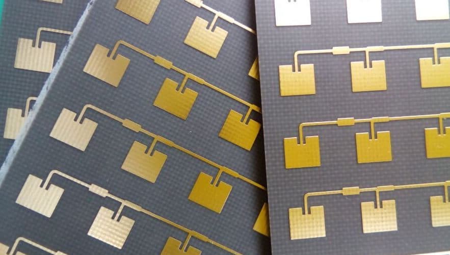
- Rogers RO4000 Series – High frequency circuit substrates with PTFE composites. Low dielectric loss.
- Ceramics – Aluminum oxide, aluminum nitride. Exceptional thermal conductivity. Used in high power and RF circuits.
- PIC/Kevlar – Woven aramid fiber/epoxy composites. Used where high strength and stiffness is required.
Copper Foil
Copper foil, ranging from 0.5 oz (18 μm) to 2 oz (70 μm) thickness is laminated to the substrate to form copper layers. The foil is etched to form PCB traces.
Multilayer Construction
Multiple rigid substrates with copper foils are laminated together under heat and pressure to form a multi-layer board. Adhesives bond the layers. Plated through holes provide connections between layers.
Common Layer Stackups
| Stackup | Description |
|---|---|
| 2 Layer | Single substrate with copper on both sides |
| 4 Layer | Two substrates bonded together with copper on the outer sides |
| 6 Layer | Three substrates bonded together with copper on the outer sides |
| 8+ Layer | Four or more substrates bonded, with alternating copper layers |
More layers allow complex interconnections in high density PCBs.
Solder Mask and Silkscreen
Solder mask is a thin lacquer coating applied over the copper traces for insulation and oxidation prevention. It leaves the soldering pads exposed. Silkscreen printing identifies components and markings.
Plated Finishes
Nickel/gold, tin, or other metallic plating is applied over exposed copper pads and traces to facilitate soldering and prevent oxidation.
Common Thickness
Typical rigid PCB thickness ranges from 0.4 mm (1 oz.) to 2.4 mm (6 oz.). Thicker boards are stronger and allow longer trace routing.
Rigid PCB Design and Layout
Rigid PCB layout involves placement of components and routing copper traces between component pads. Here are some key rigid PCB design considerations:
Component Placement
Optimal component placement minimizes trace lengths and maximizes routing efficiency. Both through-hole and surface mount components must be accommodated. High speed components need to be carefully placed.
Routing and Trace Layout
Trace widths are calculated based on current. Constraints like length matching, impedance control, and EMI control must be considered for traces. Trees are intelligently routed between pins.
Thermal Management
Heatsinks, thermal pads, and thermal vias help dissipate heat from high power components. Large copper planes spread heat across the board.
High Speed Design
Controlling impedance, crosstalk, reflections are critical for high speed PCBs. This involves trace dimensioning, routing, spacing, discontinuities, and ground planes.
EMC/EMI Control
Proper grounding, shielding, and physical layout techniques control electromagnetic interference in the circuit.
Stackup Planning
Layer stackup with optimal core thicknesses, prepreg, and copper weights is planned for electrical, thermal, and mechanical performance.
Fabrication and Assembly
Design for manufacturability ensures the board can be easily fabricated and assembled. Standard assembly processes are assumed.
CAD Software
PCB layout and routing is done using CAD software like Altium Designer, Eagle, KiCad, Pads, Allegro, and OrCAD.
Good PCB design minimizes layout errors and avoids costly board revisions.
Rigid PCB Fabrication and Testing
Once the board design is completed, rigid PCB fabrication and testing involves the following key steps:
Design Output
The PCB CAD tool outputs design files like Gerber and drill files for PCB production.
Lamination
Core substrates and copper foils are stacked up and laminated under heat and pressure using epoxy adhesives to bond layers together.
Drilling
High speed CNC drills make holes for through-hole component leads and vias for layer interconnection.
Copper Plating
Electrolytic copper plating deposits copper in drilled holes and on board surfaces for traces and vias.
Photolithography
A photosensitive dryfilm is laminated and imaged to form a mask pattern for copper traces. Exposed copper is etched away.
Solder Mask and Silkscreen
Solder mask epoxy is applied and cured. Silkscreen printing transfers markings onto the board.
Surface Finish
Plated nickel/gold, tin, or HASL finish is applied on exposed copper for protection and solderability.
Electrical Test
Bare boards are tested for opens, shorts, and leakage to catch any manufacturing defects.
Comparing Rigid and Flexible PCBs
Flexible printed circuit boards (flex PCBs) offer an alternate construction to rigid PCBs for some applications. Here is a comparison:
| Parameter | Rigid PCBs | Flex PCBs |
|---|---|---|
| Substrate | Thermoset composites like FR-4 | Thin polyimide film |
| Structure | Multilayer, rigid | Single or double layer, flexible |
| Circuit Density | Very high | Moderate |
| Thermal Stability | Excellent, up to 130°C | Moderate, around 105°C |
| Dielectric Constant | Higher ~4.5 | Lower ~3.4 |
| Applications | Ideal for complex, high density circuits | Better for dynamic flexing and 3D assembly |
| Cost | Lower | Higher |
In short, rigid PCBs are preferable for rigid structures and high density layouts, while flex PCBs suit dynamic and space constrained applications. The two are often combined in rigid-flex PCB designs.
Frequently Asked Questions
What are the different types of rigid PCB materials?
The most common rigid PCB substrate is FR-4 glass epoxy. Other materials like CEM-1/CEM-3 cellulose fiber/epoxy, Rogers high frequency laminates, PIC/Kevlar composites and ceramics like Aluminum Nitride are also used for specialized applications.
What is the minimum trace width and spacing possible with rigid PCBs?
High density PCBs can have trace widths and spacings down to 2-3 mils (around 0.05mm) by using a smaller trace/space capability process during fabrication.
How many copper layers can modern rigid PCBs support?
Advanced rigid PCBs can incorporate up to 12-16 copper layers or even more by bonding thin substrates together. High layer counts allow complex circuit routing.
How are components mounted on a rigid PCB?
Both through-hole and surface mount components can be used with rigid PCBs. Through-hole parts are inserted into holes and soldered. SMDs are placed on pads and reflow soldered. Some boards use mixed SMT and through-hole mounting.
What are thermal vias used for in rigid PCBs?
Thermal vias help conduct heat from inner copper layers to the board surfaces. An array of plated through hole vias fills with solder to create a thermal path for heat dissipation.


Leave a Reply