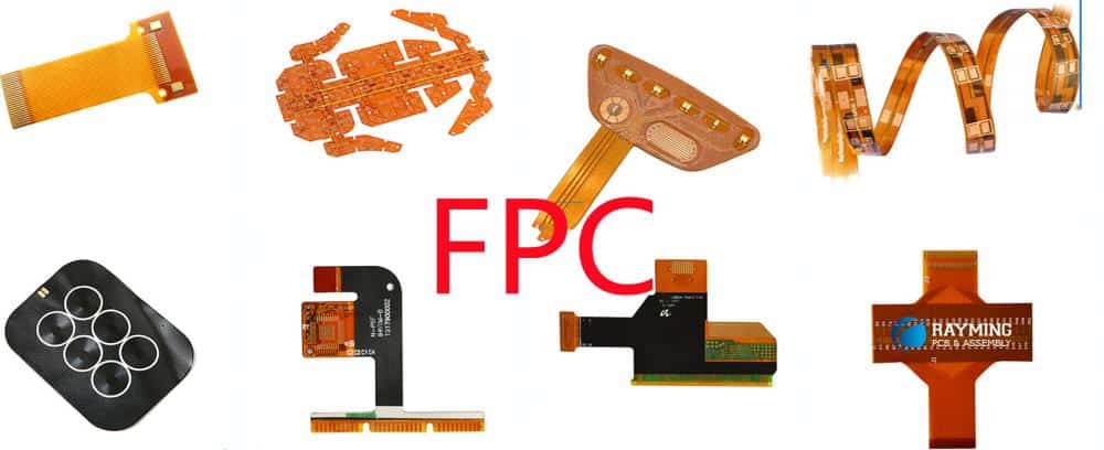
Introduction to flex PCBs
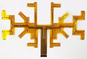
A flexible printed circuit board (flex PCB) is a type of printed circuit board made of flexible materials such as polyimide film. Flex PCBs can bend, twist, and flex without damage during use. This ability to flex makes them well-suited for applications where the circuit board needs to move or conform to a shape, such as in wearable devices, medical devices, consumer electronics, automotive electronics, and aerospace applications.
Some key properties of flex PCBs:
- Made from flexible materials like polyimide film
- Can be bent, folded, twisted without damage
- Very thin, lightweight and space saving
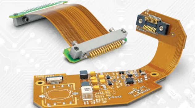
- Can be rigid sections and flex sections together
- Allows three-dimensional wiring and dense assembly
What are vias on PCBs?
Vias are plated through holes on printed circuit boards that allow connections between different layers of the PCB. On multilayer PCBs with more than 2 layers, vias make vertical interconnections between traces on different layers possible.
Some key points about vias:
- Allow connections between different layers
- Plated through holes filled with conductive material
- Used to route signals between layers on multilayer PCBs
- Allow components and traces to cross each other on different layers
- Come in different shapes: round, rectangular, castellated
Can flex PCBs have vias?
Yes, flex PCBs can have plated through hole vias just like rigid PCBs. Vias allow routing signals between different layers of the flex PCB and enable higher circuit density.
There are some considerations when using vias on flex PCBs:
- Via reliability: Vias can crack or fail with repeated bending stress. Careful design and testing is needed.
- Flexibility: Vias can reduce flexibility in the flex area. Minimize vias in high flex zones.
- Plating thickness: Thicker plating is preferred for durability. At least 25 μm copper plating.
- Annular rings: Larger annular rings around vias improve reliability. 0.2mm annular ring is typical.
- Filled vias: Filling vias improves strength. Copper filled, resin filled or conformal coating options.
Here is a comparison of flex PCB with and without vias:
| Feature | Flex PCB without Vias | Flex PCB with Vias |
|---|---|---|
| Routing density | Low | High |
| Signal layers | Single or double layer | Multilayer (4-12 layers) |
| Flexibility | Higher | Lower in via areas |
| Complexity | Simpler | More complex, advanced |
| Cost | Lower | Higher |
Via design guidelines for flex PCBs
Follow these guidelines when designing vias on flex PCBs:
- Minimize vias in areas with high bending – vias can crack.
- Use thicker copper plating – 25 μm to 35 μm for reliability.
- Have larger annular rings around vias – 0.2mm typical.
- Fill vias to improve strength – copper filled or resin filled.
- Adhere to minimum spacing between vias.
- Test board flexure life during prototyping.
- Avoid small drill sizes – 0.15mm minimum.
- Corner vias can be more durable than round vias.
- Castellated vias along edges allows more flexibility.
Pros and cons of vias on flex PCBs
Pros:
- Allow more routing layers and higher density
- Enable complex flex-rigid designs
- Allow components on both sides of the PCB
- Allow crossing of traces between layers
- Improve circuit performance with controlled impedances
Cons:
- Reduce flexibility in flex areas
- More prone to cracking failure with repeated bending
- Requires more complex PCB fabrication process
- Increases cost compared to single or double layer flex
- Requires careful engineering and testing for reliability
Applications using flex PCBs with vias
Here are some examples of products using flex PCBs with vias:
- Wearable devices – smart watches, fitness bands
- Medical devices – ultrasound probes, hearing aids
- Consumer electronics – laptops, mobile phones, cameras
- Automotive – sensors, displays, control modules
- Aerospace – control panels, engine monitoring
- Robotics – arms, joints, manipulators
For these applications, flex PCBs with vias are useful to:
- Fit in tight spaces
- Enable connections between layers
- Withstand vibration and motion
- Achieve dense, complex circuitry
Conclusion
In summary, flex PCBs can definitely incorporate plated through hole vias while maintaining flexibility. Careful design and testing is required to ensure via reliability under bending loads. Vias enable more advanced circuit architectures with multilayer flex PCBs, allowing for space and weight savings in compact devices. When designed properly, flex PCBs with vias provide an interconnect solution with reliability for demanding applications.
Frequently Asked Questions
Here are some common questions about using vias on flex PCBs:
Q1. How are vias constructed on flex PCBs?
Vias on flex PCBs are plated through holes, consisting of a hole drilled through the polyimide base material that is plated with copper to form electrical connections between layers. The polyimide material provides the flexibility while the plated copper barrel forms a stable conductive via.
Q2. Do vias reduce the flexibility of flex PCBs?
Yes, vias can reduce flexibility to some extent, especially dense areas with many vias. The rigid via barrel limits local flexibility. Careful layout and minimal use in high flex zones is advised. Castellated or corner vias impact flexibility less.
Q3. What special considerations are there for solder mask with flex PCB vias?
Solder mask pull back from vias is recommended, to prevent solder mask cracking at the rigid via barrel during flexing. A solder mask pull back of at least 0.05mm from the via pad is typical.
Q4. How are flex PCB vias tested for reliability?
Flex PCB via reliability is tested through repeated bending and cycling to failure. Testing validates the design performs to the required flex life with the chosen materials, laminates, and plating thickness.
Q5. Can flex-rigid PCBs use vias between rigid and flex sections?
Yes, carefully designed transitions with teardrop shapes allow using vias to connect between rigid sections and flexible areas on flex-rigid PCBs. This enables complex 3D routing.


Leave a Reply