Introduction to PCB Impedance Control
Printed Circuit Board (PCB) impedance control is a crucial aspect of designing high-speed electronic systems. As signal speeds increase and rise times decrease, the importance of controlling the impedance of PCB traces becomes paramount to ensure signal integrity and minimize signal distortion, reflections, and crosstalk. Impedance control is the process of designing PCB traces to have a specific characteristic impedance, typically 50 ohms or 100 ohms, to match the impedance of the components and connectors used in the system.
What is PCB Impedance?
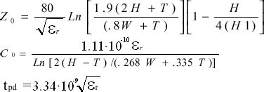
PCB impedance refers to the opposition to the flow of alternating current (AC) in a PCB trace. It is determined by the geometry of the trace, the dielectric constant of the PCB material, and the frequency of the signal. The characteristic impedance of a PCB trace is given by the formula:
Z0 = (87 / √εr) * ln(5.98h / (0.8w + t))
Where:
– Z0 is the characteristic impedance in ohms
– εr is the dielectric constant of the PCB material
– h is the height of the dielectric between the trace and the reference plane
– w is the width of the trace
– t is the thickness of the trace
Why is PCB Impedance Control Important?
PCB impedance control is crucial for several reasons:
-
Signal Integrity: Matching the impedance of PCB traces to the impedance of components and connectors ensures that signals are transmitted with minimal reflections and distortions, resulting in cleaner and more accurate signals.
-
Reduced EMI: Proper impedance control helps to minimize electromagnetic interference (EMI) by reducing the amount of ringing and overshoot on signal edges.
-
Improved Timing: Controlled impedance traces have predictable delay times, which is essential for high-speed designs where timing is critical.
-
Reliability: Impedance control helps to prevent signal integrity issues that can lead to system failures or malfunctions, improving overall reliability.
10 Tips for Advanced Requirements Impedance Control PCB Design
1. Choose the Right PCB Material
The choice of PCB material is crucial for impedance control. The dielectric constant (εr) of the material directly affects the characteristic impedance of the traces. Common PCB materials and their dielectric constants include:
| Material | Dielectric Constant (εr) |
|---|---|
| FR-4 | 4.2 – 4.5 |
| Rogers RO4003C | 3.38 |
| Rogers RO4350B | 3.48 |
| Isola IS410 | 4.11 |
When selecting a PCB material, consider the following factors:
– Dielectric constant stability over temperature and frequency
– Loss tangent (dissipation factor)
– Cost and availability
– Compatibility with the manufacturing process
2. Use Appropriate Trace Geometry
The geometry of PCB traces, including their width, thickness, and spacing, directly affects their characteristic impedance. To achieve the desired impedance, use PCB design software with built-in impedance calculators or online tools to determine the appropriate trace geometry for your chosen PCB material and layer stackup.
When designing trace geometry, consider the following:
– Trace width: Wider traces have lower impedance, while narrower traces have higher impedance.
– Trace thickness: Thicker traces have lower impedance, while thinner traces have higher impedance.
– Trace spacing: The spacing between traces and the distance to the reference plane (e.g., ground or power plane) affects the impedance.
3. Optimize Layer Stackup
The layer stackup of a PCB plays a significant role in impedance control. A well-designed stackup ensures that the desired impedance can be achieved with practical trace geometries and helps to minimize crosstalk between signals. When designing the layer stackup, consider the following:
- Use dedicated signal layers: Assign specific layers for signals, power, and ground to minimize crosstalk and simplify impedance control.
- Symmetrical stackup: A symmetrical stackup helps to balance copper distribution and minimize warpage during manufacturing.
- Reference planes: Place reference planes (ground or power) close to signal layers to provide a clear return path and control impedance.
Example 4-layer stackup:
| Layer | Material | Thickness (mil) |
|——-|———-|—————–|
| Top | Copper | 1.4 |
| Prepreg | FR-4 | 6 |
| Inner 1 | Copper | 1.4 |
| Core | FR-4 | 47 |
| Inner 2 | Copper | 1.4 |
| Prepreg | FR-4 | 6 |
| Bottom | Copper | 1.4 |
4. Route Differential Pairs Carefully
Differential signaling is commonly used in high-speed designs to improve signal integrity and reduce EMI. When routing differential pairs, it is essential to maintain the desired differential impedance and minimize skew between the positive and negative signals. Consider the following tips:
- Match trace lengths: Keep the lengths of the positive and negative traces as closely matched as possible to minimize skew.
- Maintain consistent spacing: Ensure that the spacing between the positive and negative traces remains constant along the entire length of the differential pair.
- Avoid discontinuities: Minimize the use of vias, layer transitions, and other discontinuities that can affect the impedance and cause reflections.
5. Terminate Signals Properly
Proper signal termination is essential for maintaining signal integrity and minimizing reflections. The choice of termination depends on the signal type, speed, and the components used in the system. Common termination techniques include:
- Series termination: A resistor is placed in series with the signal source to match the impedance of the trace and absorb reflections.
- Parallel termination: A resistor is placed at the end of the trace, connecting it to a reference plane (usually ground) to absorb reflections.
- Differential termination: Resistors are placed between the positive and negative signals of a differential pair and the reference plane to match the differential impedance.
6. Minimize Crosstalk
Crosstalk occurs when signals on adjacent traces interfere with each other, leading to signal integrity issues. To minimize crosstalk, consider the following:
- Increase spacing: Increase the spacing between adjacent traces to reduce the coupling between them.
- Use guard traces: Place grounded guard traces between sensitive signals to shield them from crosstalk.
- Avoid parallelism: Route traces orthogonally to each other whenever possible to minimize the coupling area.
7. Simulate and Verify Impedance
Before finalizing your PCB design, simulate and verify the impedance of critical traces using PCB design software or specialized signal integrity tools. Simulations help to identify potential issues and allow for design optimizations before manufacturing. When simulating impedance, consider the following:
- Use accurate models: Ensure that your simulations use accurate models for the PCB material, trace geometry, and components.
- Analyze multiple frequencies: Simulate the impedance at various frequencies to ensure that it remains within the desired range across the entire operating frequency range of the system.
- Verify with measurements: After manufacturing, use a time-domain reflectometer (TDR) or vector network analyzer (VNA) to measure the actual impedance of the PCB traces and compare them with the simulated values.
8. Consider the Impact of Vias
Vias are necessary for connecting traces across different layers of a PCB, but they can also introduce discontinuities that affect the impedance. To minimize the impact of vias, consider the following:
- Minimize via count: Use the minimum number of vias necessary to route the signals, as each via adds a small discontinuity.
- Optimize via geometry: The size and shape of the via can affect the impedance. Use PCB design software to optimize the via geometry for your specific stackup and materials.
- Backdrilling: In high-speed designs, consider backdrilling vias to remove the unused portion of the via stub, which can cause reflections and degrade signal integrity.
9. Collaborate with PCB Manufacturers
Collaborating closely with your PCB manufacturer is essential for ensuring that your impedance-controlled design can be manufactured reliably and cost-effectively. Consider the following:
- Communicate requirements clearly: Provide your PCB manufacturer with clear and detailed impedance requirements, including the target impedance, tolerance, and any specific materials or processes required.
- Understand manufacturing capabilities: Work with your PCB manufacturer to understand their capabilities and limitations in terms of materials, layer stackups, and trace geometries that can be reliably manufactured.
- Request impedance testing: Ask your PCB manufacturer to perform impedance testing on a sample of the manufactured boards to verify that the actual impedance meets your requirements.
10. Document and Communicate
Proper documentation and communication are critical for ensuring that your impedance-controlled PCB design is correctly implemented and can be easily maintained or modified in the future. Consider the following:
- Create a comprehensive design document: Develop a design document that includes the impedance requirements, layer stackup, trace geometries, and any other relevant information.
- Use clear naming conventions: Use descriptive and consistent naming conventions for signals, nets, and components to make the design easier to understand and navigate.
- Collaborate with your team: Regularly communicate with your design team, PCB manufacturer, and other stakeholders to ensure that everyone is aligned on the impedance control requirements and any design changes.

Frequently Asked Questions (FAQ)
1. What is the difference between single-ended and differential impedance?
Single-ended impedance refers to the impedance of a single trace with respect to a reference plane, such as ground. Differential impedance, on the other hand, refers to the impedance between two traces in a differential pair, which carry complementary signals. Differential impedance is important for maintaining signal integrity in high-speed differential signaling schemes like LVDS, HDMI, and USB.
2. How does the dielectric constant of a PCB material affect impedance?
The dielectric constant (εr) of a PCB material directly affects the characteristic impedance of the traces. A higher dielectric constant results in lower impedance, while a lower dielectric constant leads to higher impedance. When selecting a PCB material for impedance control, it is important to consider the stability of the dielectric constant over temperature and frequency to ensure consistent impedance performance.
3. What is the impact of trace surface roughness on impedance?
Trace surface roughness can affect the impedance of PCB traces, particularly at high frequencies. Rough trace surfaces can cause variations in the effective trace width and increase the skin effect losses, leading to higher impedance and increased signal attenuation. To minimize the impact of surface roughness, consider using smooth copper foils or applying surface treatments like reverse-treat electroless copper (RTEC) or very-low-profile (VLP) foils.
4. How can I minimize the impact of vias on impedance?
Vias can introduce discontinuities that affect the impedance of PCB traces. To minimize the impact of vias, consider the following:
– Minimize the number of vias used to route signals.
– Optimize the via geometry (size and shape) for your specific stackup and materials.
– Use backdrilling to remove the unused portion of the via stub in high-speed designs.
– Place vias close to the signal source or destination to minimize the length of the via stub.
– Use differential vias for differential signals to maintain symmetry and minimize mode conversion.
5. What is the role of impedance matching in high-speed PCB design?
Impedance matching is crucial in high-speed PCB design to ensure that signals are transmitted efficiently and with minimal reflections. When the impedance of a signal trace matches the impedance of the source, receiver, and any connected components, the signal can propagate without reflections, minimizing signal distortion and improving signal integrity. Proper impedance matching also helps to reduce EMI and crosstalk, as well as improve the overall reliability of the system.

Conclusion
Designing a PCB with advanced impedance control requirements is a complex task that requires careful consideration of materials, trace geometries, layer stackups, and manufacturing processes. By following the 10 tips outlined in this article and closely collaborating with your design team and PCB manufacturer, you can successfully design and manufacture high-speed PCBs with excellent signal integrity and reliability.
Remember to choose the right PCB material, optimize trace geometries and layer stackups, route differential pairs carefully, and properly terminate signals. Additionally, minimize crosstalk, simulate and verify impedance, and consider the impact of vias on your design. Finally, ensure that your design is well-documented and communicated to all stakeholders to facilitate a smooth manufacturing process and future maintenance or modifications.
By mastering the techniques of advanced impedance control, you can push the boundaries of high-speed PCB design and create cutting-edge electronic systems that perform reliably in even the most demanding applications.


Leave a Reply