Introduction to PCB X-ray Inspection
In the world of printed circuit board assembly (PCBA), ensuring the quality and reliability of the final product is of utmost importance. One crucial step in this process is PCB X-ray inspection. This non-destructive testing method allows manufacturers to examine the internal structure of PCBs, identifying potential defects and issues that may not be visible to the naked eye. In this comprehensive article, we will delve into the significance of X-ray inspection in PCBA, exploring its principles, benefits, and applications.
What is PCB X-ray Inspection?
PCB X-ray inspection is a sophisticated quality control technique that utilizes X-ray technology to create detailed images of the internal structure of printed circuit boards. By passing X-rays through the PCB, the inspection system captures high-resolution images that reveal the intricate details of the board’s components, solder joints, and other critical features.
How PCB X-ray Inspection Works
The process of PCB X-ray inspection involves the following steps:
-
X-ray Generation: An X-ray source, typically an X-ray tube, generates a beam of X-rays with a specific energy level and intensity.
-
X-ray Penetration: The X-rays pass through the PCB, interacting with the various materials and components on the board. The denser the material, the more X-rays it absorbs.
-
Image Capture: As the X-rays exit the PCB, they are captured by an X-ray detector, which converts the X-ray energy into an electrical signal.
-
Image Processing: The electrical signal is then processed by specialized software, which reconstructs the captured data into a detailed X-ray image of the PCB.
-
Analysis and Interpretation: Trained technicians or automated inspection systems analyze the X-ray images, looking for any abnormalities, defects, or deviations from the expected design.
Types of PCB X-ray Inspection Systems
There are two main types of PCB X-ray inspection systems:
-
2D X-ray Inspection: This type of system produces a two-dimensional image of the PCB, providing a top-down view of the board’s internal structure. It is suitable for detecting defects such as missing components, bridging, and solder joint issues.
-
3D X-ray Inspection: Also known as computed tomography (CT) inspection, this advanced technique creates a three-dimensional reconstruction of the PCB. It offers a more comprehensive view of the board’s internal structure, allowing for the detection of complex defects and volumetric analysis.

Benefits of PCB X-ray Inspection
Implementing X-ray inspection in the PCBA process offers numerous benefits, including:
-
Early Defect Detection: X-ray inspection allows manufacturers to identify defects early in the production process, reducing the risk of costly rework or product failures in the field.
-
Non-Destructive Testing: Unlike other inspection methods that may require cutting or cross-sectioning the PCB, X-ray inspection is a non-destructive technique. This means that the board remains intact, preserving its integrity for further testing or assembly.
-
Improved Quality and Reliability: By detecting and addressing defects before the PCB is assembled into the final product, X-ray inspection contributes to improved overall quality and reliability of the end product.
-
Cost Savings: Early defect detection and prevention of product failures translate into significant cost savings for manufacturers, as it reduces the need for rework, recalls, and warranty claims.
-
Compliance with Industry Standards: Many industries, such as aerospace, automotive, and medical devices, have stringent quality requirements. X-ray inspection helps manufacturers meet these standards by ensuring the structural integrity and reliability of their PCBs.

Applications of PCB X-ray Inspection
PCB X-ray inspection finds applications across various industries and product categories, including:
-
Consumer Electronics: X-ray inspection is widely used in the production of smartphones, tablets, laptops, and other consumer electronic devices to ensure the quality and reliability of the PCBs.
-
Automotive Electronics: With the increasing complexity of automotive electronics, X-ray inspection plays a crucial role in verifying the integrity of PCBs used in safety-critical systems such as airbags, braking systems, and autonomous driving features.
-
Aerospace and Defense: The aerospace and defense industries rely on X-ray inspection to ensure the reliability of PCBs used in aircraft, satellites, and military equipment, where failure is not an option.
-
Medical Devices: X-ray inspection is essential in the production of medical devices, such as implantable devices and diagnostic equipment, to ensure the highest level of quality and patient safety.
-
Industrial Control Systems: PCBs used in industrial control systems, such as PLCs and SCADA systems, undergo X-ray inspection to ensure their reliability in harsh operating environments.

Common Defects Detected by PCB X-ray Inspection
X-ray inspection is capable of detecting a wide range of defects in PCBs, including:
-
Solder Joint Defects: X-ray inspection can reveal solder joint issues such as voids, insufficient solder, bridging, and cold joints.
-
Component Placement Defects: It can detect misaligned, missing, or incorrectly placed components on the PCB.
-
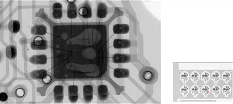
BGA and CSP Defects: X-ray inspection is particularly effective in detecting defects in ball grid array (BGA) and chip scale package (CSP) components, which are difficult to inspect visually.
-
Trace and Via Defects: X-ray inspection can identify defects in the PCB’s traces and vias, such as open circuits, short circuits, and improper connections.
-
Foreign Object Detection: It can detect the presence of foreign objects or debris within the PCB, which can cause short circuits or other reliability issues.
Automated vs. Manual PCB X-ray Inspection
PCB X-ray inspection can be performed either manually or using automated systems:
-
Manual X-ray Inspection: In manual inspection, a trained technician analyzes the X-ray images of the PCB, looking for defects and anomalies. This approach is suitable for low-volume production or when dealing with complex and unique PCB designs.
-
Automated X-ray Inspection (AXI): Automated systems use advanced algorithms and machine learning techniques to analyze X-ray images automatically. AXI systems can quickly process a large number of PCBs, making them ideal for high-volume production. They can also provide consistent and objective inspection results, reducing the risk of human error.
Integrating PCB X-ray Inspection into the PCBA Process
To maximize the benefits of X-ray inspection, it is essential to integrate it seamlessly into the PCBA process. Here are some best practices for implementing X-ray inspection:
-
Determine Inspection Points: Identify the critical points in the PCBA process where X-ray inspection should be performed, such as after solder reflow, after component placement, or before final assembly.
-
Establish Inspection Criteria: Define clear inspection criteria based on the PCB design, industry standards, and customer requirements. This includes setting acceptable tolerance levels for defects and establishing pass/fail criteria.
-
Train Personnel: Ensure that the personnel responsible for X-ray inspection are properly trained in operating the equipment, interpreting X-ray images, and identifying defects.
-
Implement Quality Control Procedures: Establish quality control procedures that outline the steps for handling defective PCBs, documenting inspection results, and implementing corrective actions.
-
Regularly Maintain and Calibrate Equipment: To ensure accurate and reliable inspection results, regularly maintain and calibrate the X-ray inspection equipment according to the manufacturer’s recommendations.
Advances in PCB X-ray Inspection Technology
PCB X-ray inspection technology continues to evolve, offering new capabilities and improved performance. Some of the latest advancements include:
-
High-Resolution Imaging: Modern X-ray inspection systems offer higher resolution imaging, enabling the detection of even the smallest defects and features on the PCB.
-
Artificial Intelligence and Machine Learning: The integration of AI and machine learning algorithms in X-ray inspection systems enhances defect detection accuracy and speeds up the inspection process.
-
Inline X-ray Inspection: Inline X-ray inspection systems allow for real-time inspection of PCBs during the assembly process, enabling immediate feedback and correction of defects.
-
3D Reconstruction and Analysis: Advanced 3D X-ray inspection systems provide detailed volumetric analysis of PCBs, allowing for the detection of complex defects and the measurement of internal features.
Frequently Asked Questions (FAQ)
- What is the difference between 2D and 3D X-ray inspection?
-
2D X-ray inspection provides a top-down view of the PCB, while 3D X-ray inspection (CT) creates a three-dimensional reconstruction of the board, offering a more comprehensive view of its internal structure.
-
Can X-ray inspection detect all types of defects in PCBs?
-
While X-ray inspection is highly effective in detecting a wide range of defects, it may not be able to detect certain types of defects, such as surface contamination or visual defects on the PCB’s exterior.
-
Is X-ray inspection safe for the PCBs being inspected?
-
Yes, X-ray inspection is a non-destructive testing method that does not damage the PCBs being inspected. The X-ray energy levels used are carefully controlled to ensure the safety of the PCBs and the operators.
-
How long does it take to perform X-ray inspection on a PCB?
-
The inspection time depends on factors such as the complexity of the PCB, the type of X-ray system used, and the inspection criteria. Automated systems can typically inspect PCBs much faster than manual inspection.
-
Can X-ray inspection be used for both prototypes and production PCBs?
- Yes, X-ray inspection is suitable for both prototype and production PCBs. It is particularly valuable for prototypes, as it allows for early identification and correction of design or manufacturing issues before mass production begins.
Conclusion
PCB X-ray inspection is a critical quality control tool in the PCBA process, ensuring the structural integrity, reliability, and performance of printed circuit boards. By detecting defects early in the manufacturing process, X-ray inspection helps manufacturers reduce costs, improve product quality, and meet stringent industry standards. As technology continues to advance, X-ray inspection systems are becoming more sophisticated, offering higher resolution imaging, automated defect detection, and 3D analysis capabilities. Integrating X-ray inspection into the PCBA process is essential for manufacturers aiming to deliver high-quality, reliable electronic products to their customers.
References
- IPC-A-610: Acceptability of Electronic Assemblies
- IPC-7095: Design and Assembly Process Implementation for BGAs
- IPC-7093: Design and Assembly Process Implementation for Bottom Termination Components
- IPC-9252: Requirements for Electrical Testing of Unpopulated Printed Boards
Word count: 1,847 words


Leave a Reply