Introduction
Printed circuit boards (PCBs) form the backbone of all electronic devices and equipment. From smartphones to medical devices to space satellites, PCBs provide the necessary electrical connections between components that allow the overall system to function. While traditionally rigid, new flexible PCB (FPCB) technology is enabling smaller, lighter, and more versatile electronic designs. This article will examine what makes flexible PCBs unique, their manufacturing process, applications, and future outlook.
What is a Flexible PCB?
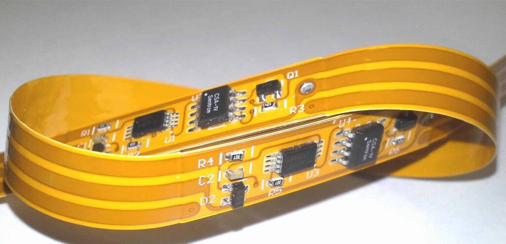
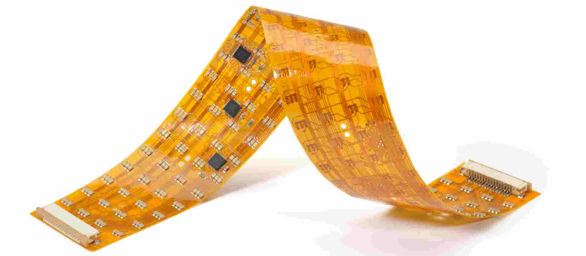
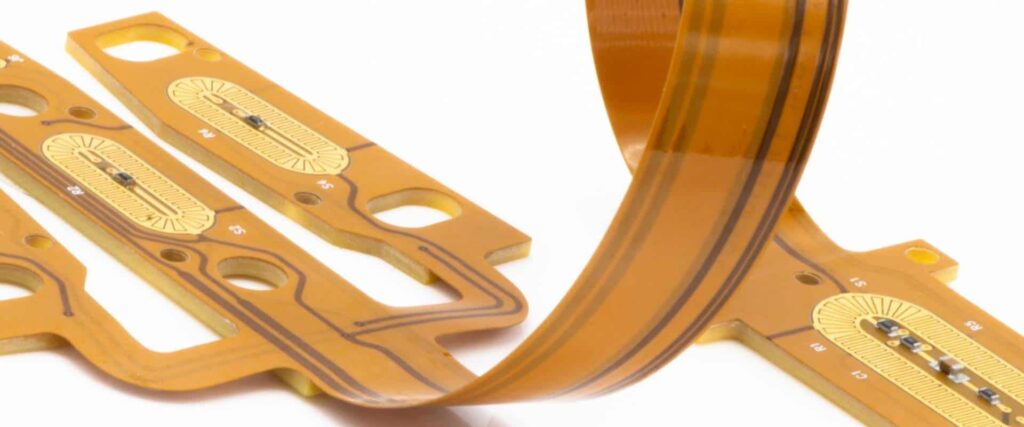
A flexible PCB is a variant of the standard PCB that utilizes a flexible, bendable substrate material rather than traditional rigid FR-4 fiberglass. The substrate provides the base layer upon which conductive copper traces are patterned to create the electrical wiring between components. While rigid PCBs use woven glass-reinforced epoxy laminate for the substrate, flexible PCBs rely on thin plastic films like polyimide (Kapton), polyester (PET), or polyvinyl chloride (PVC). This gives the board ability to flex and bend dynamically without cracking or breaking the internal traces.
Key Characteristics
- Thin, lightweight construction with thickness around 0.1-0.3mm
- Bend radius can be under 2mm allowing tight folds and wraps
- High chemical, abrasion, and temperature resistance
- Simple layer count, usually 1-4 layers
- Fine trace/space resolution down to 50/50μm
- Can be rigid sections and flex areas on same board
Benefits Over Rigid PCBs
- Conforms to challenging spaces and moving parts
- Reduces wiring/cabling needs
- Enables compact, thinner products
- Withstands vibration, shock, and flexing
- Lower weight than glass-reinforced boards
- Allows creative, efficient industrial designs
Flexible PCB Construction and Materials
While offering the ability to bend, flexible PCBs adhere to the same basic construction standards and materials as their rigid counterparts when it comes to traces, layers, and components.
Substrate Materials
The flexible plastic substrate provides the base upon which the conductive layers are built up. Polyimide films like Kapton from DuPont are most common, but other options include polyester (PET), polyethylene naphthalate (PEN), polyvinyl chloride (PVC), and polyurethane. Polyimide offers the best temperature resistance. Minimum bend radius ranges from 2mm to 10mm.
Conductive Layers
The circuit traces that carry current between components are typically made of copper foil, similar to rigid boards. Rolled annealed copper with adhesive promotes trace durability. Common thicknesses range from 1⁄2 oz (17μm) to 2 oz (70μm). Etching defines the trace patterns.
Dielectric Layers
Dielectric acrylic or polyimide layers electrically isolate between conductive layers in multilayer flex boards. Adhesives bond the layers. Flex boards typically have 1-4 layers.
Coverlay and Solder Mask
Liquid photoimageable (LPI) solder masks protect metal traces from environmental damage while preventing shorts. Flexible solder mask materials include acrylic, urethane, and silicone. Coverlay refers to the protective top layer overlaying the outer surface.
Stiffeners and Backing Layers
For areas requiring rigid sections, additional stiffener materials are added like aluminum, steel, or high-Tg thermoset polymers. Backing layers also increase rigidity.
Components and Finish
SMT components mount to the surface while connectors or molded flex cabling interface along the edges. Immersion silver, immersion tin, and gold electroplating provide surface finish.
Flexible PCB Fabrication Process
Fabricating flexible PCBs requires specialized methods to manufacture the thin, bendable circuit boards. Here are the key steps:
1. Substrate Preparation
The process starts with laminating sheets of the flexible substrate material like Kapton or PET into a continuous roll. Pretreating promotes adhesive bonding.
2. Conductive Layer Addition
Copper foil is laminated onto the substrate with adhesive bonding. For multilayer boards, additional alternating layers of dielectric and copper are added.
3. Imaging and Etching
A photoresist layer is deposited on the copper layers and imaged to form a mask. Etching removes exposed copper, leaving the desired circuit trace patterns.
4. Dielectric Layer Lamination
For multilayer flex boards, layers are aligned and laminated with epoxy dielectric films in between. Drilling forms vias between layers.
5. Surface Finish
Immersion plating with silver, tin, or gold enhances solderability and protects copper traces from oxidation and corrosion.
6. Solder Mask and Silkscreen
LPI solder mask is applied for insulation and selective trace exposure. Silkscreen printing provides markings.
7. Testing and Singulation
Electrical testing validates proper function. Routed patterns are separated into individual boards.
Flexible PCB Applications
Thanks to their thin, lightweight, and bendable traits, flexible PCBs open up some unique application possibilities that are challenging or impossible with rigid technology.
Wearable Electronics
For smartwatches, fitness bands, health monitors, and electronic textiles, flexible circuits easily conform to the curves of the human body. Light weight keeps overall product mass low.
Medical Electronics
In medical devices like hearing aids and digital imaging catheters, flexible PCBs fold up tightly to fit into ultra-compact form factors. They also help reduce patient discomfort.
Robotics and UAVs
The dynamic bending movements of robotic arms and joints are suited for flex PCBs. Their vibration resistance also handles the rigors of drones and unmanned vehicles.
Automotive Electronics
Dashboard displays, sensors, lighting, and in-vehicle infotainment systems benefit from thin, rugged flexible circuits that integrate discretely.
Consumer Electronics
Mobile phones, tablets, cameras, and portables use flex PCBs for cable connections. Tight bend radii accommodate edge wrapping and folding inside tight casings.
Aerospace and Defense
Rugged yet lightweight flexible circuits meet military and avionics standards while enduring vibration, shock, temperature swings, and repeated flexing.
Future Outlook
Flexible PCB technology will continue opening up new horizons in electronic product design. Here are some trends to watch:
- Extreme miniaturization enabling micro-scale flex circuits for medical implants, ingestible devices, nanotech.
- Development of stretchable circuits that maintain conductivity under high elongation for wearable applications.
- Higher layer counts, densities, and thinner constructions unlocking new capabilities.
- Integration of flexible PCBs with 3D printing for customized smart products.
- Growth in automotive electronics usage for vehicle sensors and lighting applications.
- Advancements in flexible/rigid PCB hybrids combining both technologies on same board.
As material science and manufacturing techniques continue to evolve, flexible PCBs will provide the backbone of ever-smaller and innovative electronic circuits and products.
FAQs
Here are some frequently asked questions about flexible PCB technology:
Q: What are some key differences between flex PCBs and rigid PCBs?
A: The main differences are the flexible substrate material rather than glass-reinforced rigid laminate, overall thinner profile, simpler layer counts, and ability to bend dynamically without cracks or breaks.
Q: Does flex PCB technology support high-density designs?
A: While fine features around 50μm lines/spaces are possible, high layer counts above 8-10 remain challenging compared to rigid boards. Flex PCBs excel in simpler, lower density circuits.
Q: What types of components can be used on flexible PCBs?
A: SMT chips and passive components are commonly used along with connectors or cables. Given the flexible nature, large through-hole parts or tall components can impose mechanical challenges.
Q: How many bend cycles can a flexible PCB withstand?
A: Many flex PCBs can endure over 1 million dynamic bend cycles before traces may weaken and eventually fracture. This makes them ideal for moving, twisting applications.
Q: What are some limitations or disadvantages of flexible circuit boards?
A: Limitations include lower layer counts than rigid technology, more costly materials involved, challenges with dense fine pitch ICs, and lack of rigidity which may necessitate stiffener add-ons.


Leave a Reply