Introduction to PCBA Drawing Requirements
Printed Circuit Board Assembly (PCBA) is a crucial process in the manufacturing of electronic devices. It involves assembling various components onto a printed circuit board (PCB) to create a functional electronic system. To ensure the success of the PCBA process, it is essential to have accurate and comprehensive assembly drawings that provide clear instructions to the manufacturing team.
In this article, we will explore the basic requirements for PCBA drawing, including the essential elements, formatting guidelines, and best practices. By understanding and adhering to these requirements, you can create assembly drawings that facilitate efficient and error-free PCBA processes.
What is a PCBA Drawing?
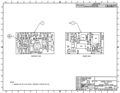
A PCBA drawing, also known as an assembly drawing, is a detailed visual representation of how electronic components should be assembled onto a PCB. It provides a clear and concise guide for the manufacturing team, ensuring that the components are placed accurately and the assembly process is carried out correctly.
PCBA drawings typically include information such as:
- Component placement and orientation
- Solder pad sizes and shapes
- Silkscreen labels and markings
- Assembly notes and instructions
- Bill of Materials (BOM)
These drawings serve as a critical communication tool between the design team and the manufacturing team, helping to minimize errors, reduce assembly time, and improve overall product quality.

Key Elements of a PCBA Drawing
To create an effective PCBA drawing, several key elements must be included. These elements provide the necessary information for the manufacturing team to accurately assemble the PCB. Let’s take a closer look at each of these elements:
1. PCB Outline and Dimensions
The PCB outline and dimensions are the foundation of the PCBA drawing. They define the physical size and shape of the PCB, including any cutouts, holes, or unique features. The dimensions should be clearly labeled, typically in millimeters or inches, and should include tolerances where applicable.
2. Component Placement and Orientation
One of the most critical aspects of a PCBA drawing is the accurate placement and orientation of components on the PCB. Each component should be clearly identified, typically using its reference designator (e.g., R1, C2, U3), and its location should be specified using coordinates or a grid system.
In addition to placement, the orientation of polarized components, such as electrolytic capacitors, diodes, and ICs, must be clearly indicated. This is often done using a silkscreen marking, such as a dot or a notch, to denote the correct orientation.
3. Solder Pad Sizes and Shapes
Solder pads are the conductive areas on the PCB where components are attached. The PCBA drawing should specify the size and shape of each solder pad, ensuring that they are compatible with the component leads or contacts.
Solder pad sizes are typically provided in a table or a separate document, such as a land pattern chart. This information is crucial for creating the solder stencil and ensuring proper solder joint formation during the assembly process.
4. Silkscreen Labels and Markings
Silkscreen labels and markings are text and symbols printed on the PCB surface to provide additional information and guidance for the assembly process. These markings can include:
- Component reference designators
- Polarity indicators
- Test points
- Mounting holes
- Fiducial markers
The PCBA drawing should clearly specify the location, size, and content of each silkscreen label and marking. It is essential to ensure that the markings are legible and do not interfere with the component placement or soldering process.
5. Assembly Notes and Instructions
In addition to the visual elements, a PCBA drawing should include assembly notes and instructions to provide further guidance to the manufacturing team. These notes can cover various aspects of the assembly process, such as:
- Special handling requirements for sensitive components
- Torque specifications for mounting hardware
- Connector mating instructions
- Conformal coating application guidelines
Assembly notes should be clear, concise, and easily understandable by the manufacturing team. They should be placed in a prominent location on the drawing, typically near the title block or in a separate notes section.
6. Bill of Materials (BOM)
A Bill of Materials (BOM) is a comprehensive list of all the components required for the PCBA. It includes information such as the component reference designator, manufacturer part number, description, and quantity.
While the BOM is often provided as a separate document, it is essential to ensure that it aligns with the information presented in the PCBA drawing. Any discrepancies between the BOM and the drawing can lead to confusion and assembly errors.

PCBA Drawing Formatting Guidelines
In addition to the key elements, there are several formatting guidelines that should be followed to ensure the clarity and consistency of PCBA drawings. These guidelines help to standardize the presentation of information, making it easier for the manufacturing team to interpret and follow the assembly instructions.
1. Title Block and Revision Control
Every PCBA drawing should include a title block that contains essential information about the drawing, such as:
- Drawing title and number
- Revision level and date
- Company name and logo
- Drawn by and checked by initials
- Scale and sheet number
The title block should be located in a consistent position on each drawing sheet, typically in the lower right corner. Revision control is crucial for tracking changes to the drawing and ensuring that the manufacturing team is always working with the most up-to-date version.
2. Layer Identification and Color Coding
PCBA drawings often include multiple layers, such as the top and bottom copper layers, silkscreen, and solder mask. To help differentiate between these layers, a clear layer identification system should be used.
Color coding is a common method for distinguishing layers, with each layer assigned a specific color. For example:
- Top copper layer: Red
- Bottom copper layer: Blue
- Silkscreen: Yellow
- Solder mask: Green
The layer colors should be consistent throughout the drawing set and should be defined in a legend or key on each drawing sheet.
3. Font Selection and Sizing
The choice of font and text size can significantly impact the readability of a PCBA drawing. It is essential to use a clear, legible font that is easy to read even when the drawing is reduced in size.
Some commonly used fonts for PCBA drawings include:
- Arial
- Helvetica
- Verdana
- Tahoma
Text sizes should be chosen based on the importance of the information and the available space on the drawing. Key information, such as component reference designators and dimensions, should be larger and more prominent than secondary details.
4. Line Weights and Styles
Consistent use of line weights and styles can help to improve the clarity and organization of a PCBA drawing. Different line weights can be used to emphasize certain features or to distinguish between different types of information.
For example:
- Thick lines for the PCB outline and major components
- Medium lines for component outlines and solder pads
- Thin lines for dimensions and annotations
Line styles, such as solid, dashed, or dotted lines, can also be used to convey specific information. For instance, a dashed line may be used to represent a hidden edge or a cutout in the PCB.
5. Drawing Scale and Units
The scale and units used in a PCBA drawing should be clearly stated on each drawing sheet. This information helps the manufacturing team to interpret the dimensions and sizes accurately.
The most common scale for PCBA drawings is 1:1, meaning that the drawing represents the actual size of the PCB. However, larger or more complex designs may require a different scale, such as 2:1 or 4:1.
The units of measurement should also be specified, typically in millimeters or inches. It is essential to use a consistent unit throughout the drawing set to avoid confusion and errors.

Best Practices for PCBA Drawing Creation
Creating effective PCBA drawings requires not only adherence to the basic requirements and formatting guidelines but also the application of best practices. These practices help to ensure that the drawings are accurate, complete, and easily understandable by the manufacturing team.
1. Use a Consistent Template
Developing and using a consistent template for PCBA drawings can help to streamline the creation process and ensure uniformity across multiple projects. The template should include all the necessary elements, such as the title block, layer identification, and font specifications.
By using a template, designers can focus on the specific details of each drawing rather than spending time setting up the basic structure and formatting.
2. Collaborate with the Manufacturing Team
Effective communication between the design team and the manufacturing team is essential for successful PCBA. Designers should collaborate with the manufacturing team throughout the drawing creation process to ensure that the drawings meet their needs and expectations.
This collaboration can help to identify potential issues early in the process, such as component placement challenges or assembly constraints. By working together, the design and manufacturing teams can develop solutions that optimize the assembly process and improve overall product quality.
3. Conduct Thorough Reviews and Verifications
Before releasing PCBA drawings to the manufacturing team, it is crucial to conduct thorough reviews and verifications. This process should involve multiple stakeholders, including designers, engineers, and quality control specialists.
Some key aspects to review and verify include:
- Component placement and orientation
- Solder pad sizes and shapes
- Silkscreen labels and markings
- Assembly notes and instructions
- BOM accuracy and alignment with the drawing
By catching and correcting errors and inconsistencies during the review process, designers can help to minimize the risk of assembly issues and delays.
4. Maintain Accurate Documentation and Revision Control
Accurate documentation and revision control are essential for ensuring that the manufacturing team always has access to the most up-to-date and correct PCBA drawings. Designers should maintain a clear and organized system for tracking drawing revisions, including:
- Assigning unique revision numbers or letters
- Recording the date and reason for each revision
- Archiving previous versions for reference
When issuing a new revision, it is important to communicate the changes clearly to the manufacturing team and ensure that all outdated drawings are removed from circulation.
5. Continuously Improve and Optimize
PCBA drawing creation is an ongoing process that requires continuous improvement and optimization. Designers should actively seek feedback from the manufacturing team and other stakeholders to identify areas for enhancement.
This feedback can help to refine drawing elements, improve formatting and presentation, and streamline the overall assembly process. By continuously improving PCBA drawings, designers can contribute to better product quality, reduced assembly times, and increased customer satisfaction.
Table: PCBA Drawing Checklist
| Category | Element | Included |
|---|---|---|
| PCB Outline and Dimensions | Board size and shape | ☐ |
| Cutouts and holes | ☐ | |
| Dimensional tolerances | ☐ | |
| Component Placement and Orientation | Reference designators | ☐ |
| Placement coordinates or grid | ☐ | |
| Polarity markers | ☐ | |
| Solder Pad Sizes and Shapes | Pad dimensions | ☐ |
| Pad shapes | ☐ | |
| Land pattern chart | ☐ | |
| Silkscreen Labels and Markings | Component reference designators | ☐ |
| Polarity indicators | ☐ | |
| Test points and fiducials | ☐ | |
| Assembly Notes and Instructions | Special handling requirements | ☐ |
| Torque specifications | ☐ | |
| Connector mating instructions | ☐ | |
| Bill of Materials (BOM) | Component reference designators | ☐ |
| Manufacturer part numbers | ☐ | |
| Quantities | ☐ | |
| Formatting | Title block and revision control | ☐ |
| Layer identification and color coding | ☐ | |
| Font selection and sizing | ☐ | |
| Line weights and styles | ☐ | |
| Drawing scale and units | ☐ |
Frequently Asked Questions (FAQ)
1. What software is commonly used for creating PCBA drawings?
Various software packages are used for creating PCBA drawings, including:
- Autodesk Eagle
- Altium Designer
- KiCad
- Cadence OrCAD
- Mentor Graphics PADS
These software tools provide comprehensive features for designing PCBs and generating assembly drawings, including component libraries, routing capabilities, and automated documentation generation.
2. What file formats are typically used for sharing PCBA drawings?
PCBA drawings are typically shared in the following file formats:
- Gerber files (RS-274X) for individual layers
- ODB++ (Open Database) for full assembly data
- PDF (Portable Document Format) for visual reference and printing
- DXF (Drawing Exchange Format) for exporting to other CAD systems
It is essential to consult with the manufacturing team to determine their preferred file formats and ensure compatibility with their systems.
3. How can I ensure the accuracy of my PCBA drawings?
To ensure the accuracy of your PCBA drawings, consider the following tips:
- Use a consistent and reliable component library
- Double-check component placement and orientation
- Verify solder pad sizes and shapes against component datasheets
- Conduct thorough reviews and verifications with multiple stakeholders
- Collaborate with the manufacturing team to identify potential issues
By following these practices and maintaining attention to detail, you can minimize the risk of errors and inconsistencies in your PCBA drawings.
4. What should I do if I need to make changes to a PCBA drawing after it has been released?
If you need to make changes to a PCBA drawing after it has been released, follow these steps:
- Create a new revision of the drawing with an updated revision number or letter
- Clearly document the changes made and the reason for the revision
- Communicate the changes to the manufacturing team and other relevant stakeholders
- Ensure that all outdated versions of the drawing are removed from circulation
- Update any associated documentation, such as the BOM or assembly instructions
By following a structured revision control process, you can ensure that changes are implemented smoothly and that everyone is working with the most up-to-date information.
5. How can I optimize my PCBA drawings for manufacturability?
To optimize your PCBA drawings for manufacturability, consider the following tips:
- Collaborate with the manufacturing team to understand their capabilities and constraints
- Use standard component sizes and packages whenever possible
- Provide clear and concise assembly notes and instructions
- Ensure adequate spacing between components for ease of assembly
- Consider the use of fiducial markers and test points to aid in the assembly process
- Continuously seek feedback from the manufacturing team and incorporate their suggestions
By designing with manufacturability in mind and maintaining open communication with the manufacturing team, you can create PCBA drawings that facilitate efficient and reliable assembly processes.
Conclusion
PCBA drawings play a critical role in the success of electronic product manufacturing. By understanding and adhering to the basic requirements, formatting guidelines, and best practices outlined in this article, designers can create clear, accurate, and comprehensive assembly drawings that streamline the PCBA process.
Key elements of a PCBA drawing include the PCB outline and dimensions, component placement and orientation, solder pad sizes and shapes, silkscreen labels and markings, assembly notes and instructions, and the bill of materials. Proper formatting, including the use of consistent templates, layer identification, and font selection, helps to ensure the clarity and readability of the drawings.
To optimize the PCBA drawing creation process, designers should collaborate with the manufacturing team, conduct thorough reviews and verifications, maintain accurate documentation and revision control, and continuously seek opportunities for improvement and optimization.
By investing time and effort into creating high-quality PCBA drawings, designers can contribute to faster assembly times, fewer errors, and improved overall product quality. As the electronics industry continues to evolve, the importance of effective PCBA drawing practices will only continue to grow, making it essential for designers to stay up-to-date with the latest requirements and best practices.


Leave a Reply