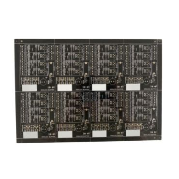
What is a Semiconductor PCB?
A semiconductor PCB is a specialized type of printed circuit board that incorporates semiconductor components, such as transistors, diodes, and integrated circuits (ICs). These components are mounted on a non-conductive substrate, typically made of materials like FR-4, ceramic, or polyimide. The substrate is then coated with a conductive layer, usually copper, which is etched to create the desired circuit pattern. This pattern allows electrical signals to flow between the components, enabling the device to perform its intended functions.
Key Features of Semiconductor PCBs
Semiconductor PCBs exhibit several unique features that set them apart from traditional PCBs:
- High component density: Semiconductor PCBs can accommodate a large number of components in a compact space, making them ideal for miniaturized devices.
- Enhanced thermal management: The substrate materials used in semiconductor PCBs often have excellent thermal conductivity, allowing for efficient heat dissipation.
- Improved signal integrity: The careful design and layout of semiconductor PCBs minimize signal interference and ensure optimal performance.
- Flexibility in design: Semiconductor PCBs can be customized to meet specific device requirements, enabling a wide range of applications.
Types of Semiconductor PCBs
Semiconductor PCBs can be classified into several categories based on their construction, material, and application:
1. Rigid PCBs
Rigid semiconductor PCBs are the most common type, featuring a solid, non-flexible substrate. They are known for their durability and reliability, making them suitable for a wide range of applications, including:
- Consumer electronics (e.g., smartphones, tablets, laptops)
- Industrial control systems
- Automotive electronics
- Medical devices
2. Flexible PCBs
Flexible semiconductor PCBs, also known as flex PCBs, use a flexible substrate material, such as polyimide or polyester. This allows the PCB to bend and conform to various shapes, making them ideal for applications that require compact packaging or movable parts. Some common applications include:
- Wearable devices
- Aerospace and military equipment
- Robotics
- Medical implants
3. Rigid-Flex PCBs
Rigid-flex semiconductor PCBs combine the benefits of both rigid and flexible PCBs. They consist of rigid sections connected by flexible sections, allowing for three-dimensional packaging and improved reliability. Applications for rigid-flex PCBs include:
- Aerospace and defense systems
- Automotive electronics
- Medical devices
- High-end consumer electronics
4. High-Frequency PCBs
High-frequency semiconductor PCBs are designed to handle high-speed signals and minimize signal loss and interference. They often use specialized substrate materials with low dielectric constants and dissipation factors, such as PTFE (polytetrafluoroethylene) or Rogers materials. High-frequency PCBs are commonly used in:
- Wireless communication devices (e.g., 5G networks)
- Radar systems
- Satellite communication equipment
- High-speed digital circuits

Semiconductor PCB Manufacturing Process
The manufacturing process for semiconductor PCBs involves several critical steps to ensure the highest quality and reliability:
-
Design and Layout: The PCB design is created using specialized software, taking into account factors such as component placement, signal routing, and thermal management.
-
Substrate Preparation: The substrate material is cut to the desired size and shape, and any necessary holes are drilled.
-
Copper Cladding: A thin layer of copper is laminated onto the substrate using heat and pressure.
-
Photoresist Application: A light-sensitive photoresist is applied to the copper layer and exposed to UV light through a photomask, which contains the circuit pattern.
-
Etching: The unexposed copper is removed using a chemical etching process, leaving behind the desired circuit pattern.
-
Soldermask and Silkscreen: A soldermask is applied to protect the copper traces, and a silkscreen is added for component labeling and identification.
-
Component Placement: The semiconductor components are placed on the PCB using automated pick-and-place machines or manual assembly.
-
Soldering: The components are soldered to the PCB using various techniques, such as wave soldering, reflow soldering, or hand soldering.
-
Inspection and Testing: The completed PCB undergoes rigorous inspection and testing to ensure proper functionality and adherence to quality standards.

Applications of Semiconductor PCBs
Semiconductor PCBs find applications in a wide range of industries and devices, thanks to their versatility and performance. Some notable applications include:
1. Consumer Electronics
Semiconductor PCBs are the backbone of modern consumer electronics, such as:
– Smartphones and tablets
– Laptops and desktop computers
– Smart home devices (e.g., smart speakers, thermostats, security systems)
– Gaming consoles and peripherals
– Wearable devices (e.g., smartwatches, fitness trackers)
2. Automotive Electronics
The automotive industry heavily relies on semiconductor PCBs for various systems and components, including:
– Engine control units (ECUs)
– Infotainment systems
– Advanced driver assistance systems (ADAS)
– Electric vehicle power management
– Sensors and actuators
3. Medical Devices
Semiconductor PCBs play a crucial role in medical devices, enabling precise and reliable operation:
– Diagnostic imaging equipment (e.g., MRI, CT scanners)
– Patient monitoring systems
– Implantable devices (e.g., pacemakers, neurostimulators)
– Surgical instruments
– Laboratory equipment
4. Industrial Automation and Control
Semiconductor PCBs are essential for industrial automation and control systems, such as:
– Programmable logic controllers (PLCs)
– Human-machine interfaces (HMIs)
– Sensors and transducers
– Motor drives and power electronics
– Robotics and motion control
5. Aerospace and Defense
Semiconductor PCBs are used in various aerospace and defense applications, where reliability and performance are crucial:
– Avionics systems
– Satellite communication equipment
– Radar and sonar systems
– Guidance and navigation systems
– Military communication devices

Future Trends in Semiconductor PCBs
As technology continues to advance, semiconductor PCBs are expected to evolve to meet the growing demands of modern devices. Some notable trends include:
-
Miniaturization: The push for smaller, more compact devices will drive the development of even higher-density semiconductor PCBs with advanced packaging techniques, such as 3D integration and system-in-package (SiP) solutions.
-
High-Speed Communications: With the proliferation of 5G networks and the increasing demand for high-speed data transmission, semiconductor PCBs will need to support higher frequencies and minimize signal integrity issues.
-
Advanced Materials: The development of new substrate materials with improved thermal, electrical, and mechanical properties will enable semiconductor PCBs to meet the challenges of emerging applications, such as high-power electronics and harsh environment operation.
-
Sustainable Manufacturing: As environmental concerns gain prominence, the semiconductor PCB industry will focus on developing eco-friendly manufacturing processes and materials, such as halogen-free substrates and lead-free solders.
-
Artificial Intelligence and Machine Learning: The integration of AI and ML capabilities into semiconductor PCBs will enable the development of smart, adaptive devices that can learn and optimize their performance over time.
Frequently Asked Questions (FAQ)
- What is the difference between a semiconductor PCB and a regular PCB?
A semiconductor PCB incorporates semiconductor components, such as transistors, diodes, and integrated circuits, while a regular PCB primarily uses passive components, like resistors, capacitors, and inductors. Semiconductor PCBs often require specialized substrate materials and manufacturing processes to accommodate the unique requirements of semiconductor components.
- Can semiconductor PCBs be repaired or reworked?
Yes, semiconductor PCBs can be repaired or reworked, but it requires specialized equipment and expertise. Common repair techniques include component replacement, trace repair, and jumper wire additions. However, the complexity of the repair depends on the PCB design, component density, and the nature of the damage.
- How do I choose the right type of semiconductor PCB for my application?
Choosing the right type of semiconductor PCB depends on several factors, such as the intended application, environmental conditions, performance requirements, and budget. Consider the following aspects:
– Rigid, flexible, or rigid-flex construction
– Substrate material properties (e.g., thermal conductivity, dielectric constant)
– Component density and packaging requirements
– Signal integrity and high-frequency performance needs
– Reliability and durability expectations
Consult with a semiconductor PCB manufacturer or design expert to determine the best solution for your specific application.
- What are the challenges in manufacturing semiconductor PCBs?
Manufacturing semiconductor PCBs presents several challenges, including:
– Achieving high component density while maintaining signal integrity
– Managing thermal dissipation and preventing component overheating
– Ensuring precise alignment and placement of small, delicate components
– Minimizing contamination and defects during the fabrication process
– Adapting to rapidly changing technology and industry standards
Manufacturers must invest in advanced equipment, skilled personnel, and stringent quality control measures to overcome these challenges and produce high-quality semiconductor PCBs.
- How can I ensure the reliability and longevity of semiconductor PCBs in my products?
To ensure the reliability and longevity of semiconductor PCBs in your products, consider the following best practices:
– Use high-quality components from reputable suppliers
– Follow best practices for PCB design, including proper signal routing, grounding, and shielding
– Perform thorough testing and validation, including environmental stress tests and accelerated life tests
– Implement robust quality control measures throughout the manufacturing process
– Provide clear guidelines for handling, storage, and assembly of the PCBs
– Monitor and analyze field performance data to identify and address any potential issues proactively
By adhering to these practices and working closely with experienced semiconductor PCB manufacturers, you can ensure the reliability and longevity of your products.
Conclusion
Semiconductor PCBs are the unsung heroes of the modern electronics industry, enabling the development of increasingly sophisticated and powerful devices. From consumer electronics and automotive systems to medical devices and aerospace applications, semiconductor PCBs provide the foundation for innovation and advancement.
As we move towards a future filled with smart, connected, and high-performance devices, the importance of semiconductor PCBs will only continue to grow. By staying at the forefront of technological advancements, such as miniaturization, high-speed communication, and advanced materials, the semiconductor PCB industry will play a crucial role in shaping the devices of tomorrow.
Whether you are an electronics engineer, a product designer, or a technology enthusiast, understanding the capabilities and potential of semiconductor PCBs is essential. By leveraging the versatility and performance of these remarkable circuit boards, we can continue to push the boundaries of what is possible and create devices that enhance our lives in countless ways.


Leave a Reply