Introduction
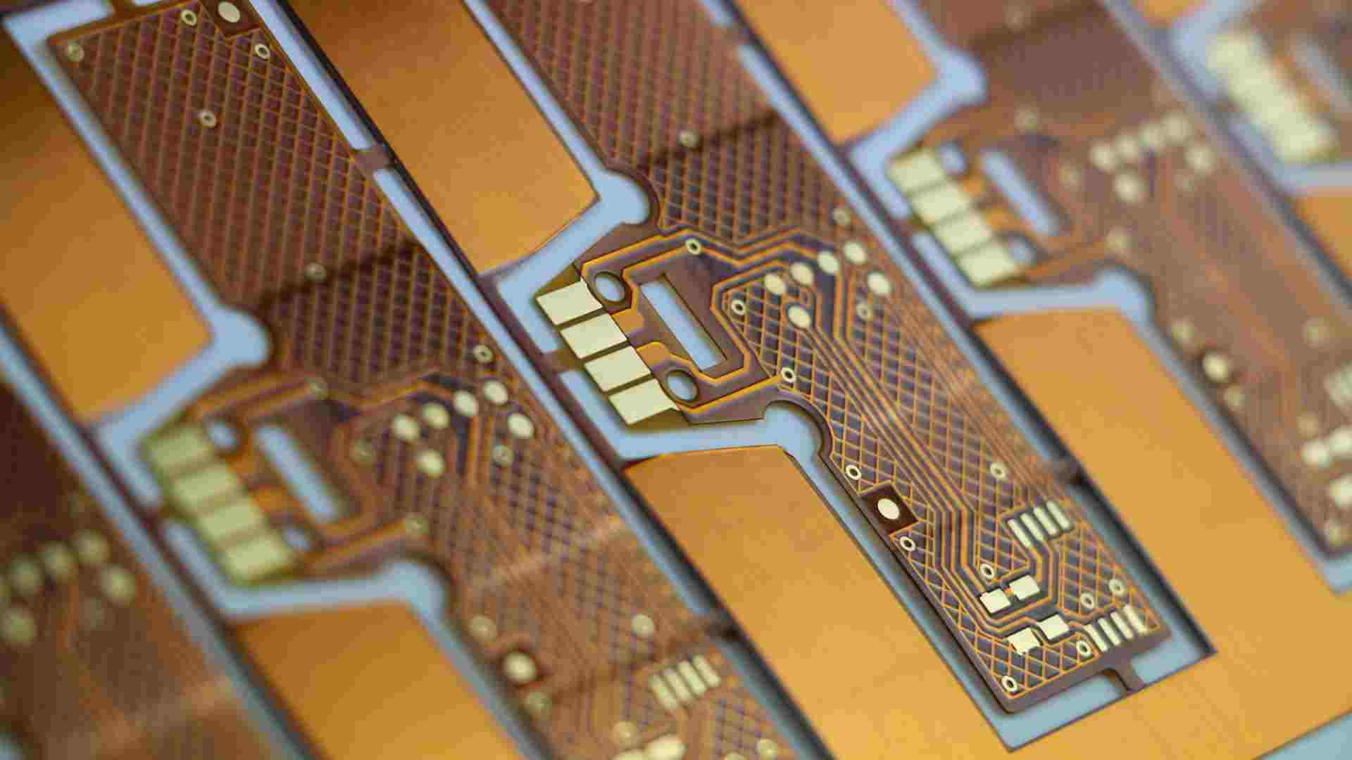
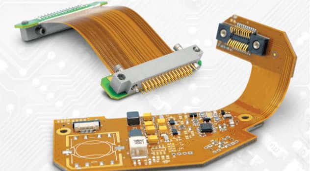
Flex-rigid PCBs, also known as rigid-flex circuits, are printed circuit boards that contain rigid sections interconnected by flexible sections. This allows the PCB to bend and flex to fit into tight spaces or move dynamically within an assembly. With both flexible and rigid portions on the same board, flex-rigid PCBs provide more functionality in a smaller footprint compared to using separate rigid and flex boards.
Altium Designer provides extensive tools for designing and manufacturing complex flex-rigid PCBs. This includes specialized features for defining flex and rigid sections, layer stackup design, component placement across rigid-flex boundaries, and generating fabrication and assembly output. With Altium’s flex-rigid design features, PCB designers can create compact and reliable circuits to meet the needs of modern electronic devices and products.
Defining Rigid-Flex Regions
The first step in designing a flex-rigid PCB in Altium is to define the rigid and flexible regions. This is done through the Flexible Region mode within the PCB panel:
Create Rigid-Flex Regions
- Enable the Flexible Region mode under the PCB panel.
- Draw solid regions to define rigid sections.
- Draw dotted lines to define flexible sections between rigid areas. Adjust line width to match flexible circuit traces.
Rigid sections can be different sizes and shapes as needed for the circuit layout. Flexible sections are typically long thin connections, but can also be wider if the final board will bend in multiple directions.
Once the regions are defined, component placement and routing can be constrained to the appropriate areas. The software ensures clearance requirements are maintained between rigid and flex sections.
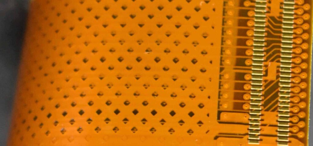
Layer Stack Management
A key aspect of flex-rigid design is managing the differences in layer stacks between rigid and flexible sections:
Adjust Layer Stacks
- Open the Layer Stack Manager under Design » Layer Stack Manager.
- Select layer sections (e.g. “Flex Region 1”) and define suitable flexible layer stackup. Typical flex stackup has 1-4 copper layers.
- Define layer stack for each rigid section with thicker substrates and more layers, typically 6-12. Match stackups at rigid-flex junctions.
- Assign electrical connections between layers (e.g. thru-hole vias, microvias).
- Review final stackup with Stackup Planner. Adjust as needed.
Careful layer stack design ensures reliable performance under bending and flexing stress. Altium provides extensive tools for managing layer stacks and connections between rigid and flex sections.
Placement and Routing
With regions defined and layer stacks configured, component placement and routing can begin:
Work Across Rigid-Flex Boundaries
- Place components onto rigid sections first, then span across flexible sections as needed.
- Assign components to Top or Bottom surface layers. Do not assign to internal flex layers.
- Route signals between components and pads. Follow clearance rules when crossing flex outlines.
- Minimize flexible routing length and avoid 90 degree bends where possible.
- Use staggered vias when routing signals between rigid sections for reliability.
Altium allows the designer flexibility to route signals across both rigid and flex regions of the PCB while following clearance constraints. This streamlines the layout process.
Design Rule Checking
Rigorous design rule checking helps identify errors and validate flex-rigid PCB layouts:
Perform Design Rule Checks
- Run Design » Rules Check to validate rules related to flex-rigid design:
- Rigid-to-flex clearance
- Flex bend radius
- Annular ring requirement
- Routing widths
- Use View » Violations to inspect specific violations
- Resolve any errors before manufacturing output
Addressing errors during design rule checking eliminates costly manufacturing issues resulting from improper rigid-flex clearance or constraints. Altium provides the flex-rigid rule checks critical for success.
Manufacturing Outputs
Altium Designer includes extensive tools for generating manufacturing and assembly outputs for flex-rigid PCBs:
Generate Fabrication and Assembly Files
- Run File » Fabrication Outputs » ODB++ to generate board fabrication data files.
- Confirm layer stackup information is included.
- Include top and bottom overlay drawings for assembly.
- Generate Files » Assembly Outputs » IPC-2581 to provide assembly documentation.
- Supply rigid-flex and stackup details in assembly drawings.
- Set File Format options to PDF/PNG/DXF as needed.
The specialized outputs allow manufacturers to clearly distinguish between rigid and flexible areas of the PCB along with layer stack information. This is essential for fabricating and assembling complex rigid-flex designs.
Benefits of Rigid-Flex PCBs
Implementing flex-rigid PCB technology with Altium Designer provides numerous advantages:
- Reduced footprint: Rigid-flex PCBs fit into tight spaces by folding and bending within an enclosure.
- Increased component density: More components can be packed onto flex boards spanning rigid sections.
- Improved reliability: Dynamic flexing reduces mechanical stress compared to connectors between separate rigid and flex boards.
- Design flexibility: Components can be placed across rigid and flex sections for easier routing.
- Lower costs: A single rigid-flex board can replace complex PCB assemblies or wire harnesses.
For products where space, weight, and reliability are critical factors, flex-rigid PCB technology enables breakthrough solutions. Altium’s robust toolset streamlines the design process.
FQA
What are the key benefits of rigid-flex PCBs?
Some of the main benefits of rigid-flex PCBs are reduced footprint from tight bending and folding, increased component density spanning rigid sections, improved reliability from dynamic flexing, design flexibility with placement across rigid and flex, and lower costs by consolidating complex assemblies onto a single board.
What are some typical applications for rigid-flex PCBs?
Flex-rigid PCBs are commonly used in portable electronics like cellphones and laptops to save space, in wearable medical devices for ergonomic designs, in aerospace systems to withstand vibration, and in robotics for motion capabilities. The ability to bend and flex makes them suitable for many applications with space, motion, or reliability constraints.
What special considerations exist for routing rigid-flex PCBs?
When routing rigid-flex PCBs, it is important to minimize routing lengths in the flex sections, avoid 90 degree bends, and provide sufficient clearances between rigid and flex. Staggered vias should be used when routing across flex sections for reliability. Sufficient bend radius should be designed in the flex areas.
What are some best practices for layer stack design of rigid-flex PCBs?
For layer stack design, use thicker substrates with more layers (6-12) in rigid sections, and thinner substrates with fewer layers (1-4) in flex sections. Match layer count between rigid and flex at junction locations. Assign electrical connections carefully between layers using vias and microvias. Model bending stress and test reliability.
How are components handled on rigid-flex PCBs in Altium?
In Altium, components should be placed primarily on the rigid sections. But they can span across flex sections as needed for routing simplicity. Components are always assigned to the Top or Bottom surface layers only, not internal flex layers. The software then ensures clearance rules are maintained at rigid-flex boundaries.


Leave a Reply