What are Microvias and Why are They Superior to Other Vias?
Microvias are an advanced type of via (vertical interconnect access) used in high-density interconnect (HDI) printed circuit boards (PCBs). Compared to traditional through-hole vias and blind/buried vias, microvias offer several advantages that make them superior for many advanced electronics applications.
A microvia is defined as a small via with a diameter less than or equal to 150 μm (6 mil) and a pad diameter less than 350 μm (14 mil). They are typically laser-drilled, allowing for precise placement and ultra-small sizes. Microvias enable higher routing density, improved signal integrity, and better thermal management compared to larger mechanically-drilled vias.
Key advantages of microvias include:
- Smaller size (down to 25 μm)
- Higher density interconnects
- Improved signal integrity
- Lower inductance and capacitance
- Better heat dissipation
- Ideal for HDI and sequential lamination
- Enable chip packaging and 3D PCB structures
The superiority of microvias lies in their ability to provide denser, higher-performance interconnects for advanced electronics, making them essential for applications like smartphones, wearables, 5G, automotive, aerospace, medical devices, and high-performance computing.
How Microvias Enable Higher Interconnect Density
One of the key advantages of microvias is their ability to provide significantly higher interconnect density compared to traditional vias. This is critical for advanced electronics that require packing more functionality into smaller form factors.
Microvias have diameters as small as 25 μm (1 mil), allowing them to be placed in much tighter pitches and in larger quantities than larger vias. For example, a typical HDI design may use microvias with 100 μm (4 mil) diameters at 200 μm (8 mil) pitch, providing an interconnect density 4-16x higher than a standard through-hole via design.
| Microvia Type | Typical Diameter | Typical Pitch | Relative Density |
|---|---|---|---|
| Through-hole | 300-500 μm | 800-1000 μm | 1x |
| Blind/buried | 150-250 μm | 500-800 μm | 2-4x |
| Microvia | 50-150 μm | 200-400 μm | 4-16x |
This increased density allows microvias to be placed directly under chips, enabling finer-pitch ball grid array (BGA) and chip-scale package (CSP) connections. It also frees up more PCB real estate for signal routing, passive components, and other features.
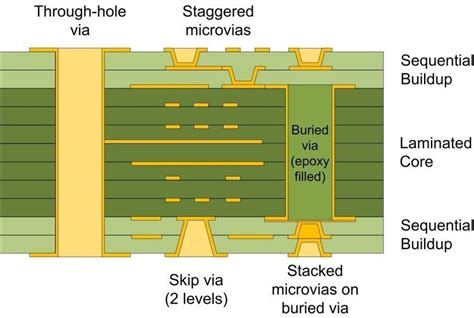
Additionally, microvias can be stacked and staggered across multiple HDI layers using sequential lamination, providing even higher interconnect density in a 3D PCB structure. This is not possible with through-hole vias and is limited with blind/buried vias.
The higher interconnect density enabled by microvias is essential for miniaturization, integration, and performance in advanced electronics, making them a superior choice over other via types.

Microvias Provide Superior Signal Integrity
Another key advantage of microvias is their ability to provide superior signal integrity compared to other via types. This is critical for high-speed, high-frequency applications where maintaining signal quality is essential.
Microvias have smaller sizes and shorter lengths than traditional vias, which reduces their electrical parasitics like inductance, capacitance, and resistance. Lower parasitics help to:
- Minimize signal distortion and attenuation
- Reduce crosstalk and electromagnetic interference (EMI)
- Enable higher signal bandwidths and data rates
- Improve impedance matching and reduce reflections
For example, a microvia with a 50 μm diameter and 100 μm length may have 75% lower inductance and 50% lower capacitance than a 250 μm through-hole via. This can significantly improve signal rise/fall times, reduce jitter, and enable higher-frequency operation.
| Via Type | Typical Inductance (@ 1 GHz) | Typical Capacitance |
|---|---|---|
| Through-hole | 1-2 nH | 0.5-1 pF |
| Blind/buried | 0.5-1 nH | 0.2-0.5 pF |
| Microvia | 0.1-0.5 nH | 0.05-0.2 pF |
Additionally, the smaller size and higher density of microvias allows for more precise control over signal routing, impedance, and return paths. This includes techniques like via-in-pad, differential pairs, and ground shielding that are more difficult or impossible with larger vias.
The superior signal integrity provided by microvias is essential for applications like high-speed digital interfaces (USB, PCIe, HDMI), RF/microwave circuits, and sensitive analog/mixed-signal designs. It helps to ensure reliable operation, reduce EMI, and meet strict signal quality requirements.

Microvias Offer Better Thermal Management
In addition to electrical advantages, microvias also offer better thermal management compared to other via types. This is important for handling higher power densities and reducing heat-related reliability issues in advanced electronics.
Microvias have smaller thermal masses and higher surface area-to-volume ratios than larger vias, which allows them to transfer heat more efficiently from hot spots to internal copper planes and external heatsinks. They can also be placed in arrays or stacked to create thermal vias with even higher heat transfer capabilities.
For example, a BGA package with a 10×10 array of 100 μm microvias can provide 2-3x more thermal conductivity than the same area filled with 4-5 through-hole vias. This can significantly reduce chip junction temperatures and improve reliability.
| Via Type | Typical Thermal Conductivity (@ 25°C) |
|---|---|
| Through-hole | 200-300 W/m-K |
| Blind/buried | 300-400 W/m-K |
| Microvia | 400-600 W/m-K |
Additionally, the smaller size and higher density of microvias allows for more precise control over thermal management in the PCB layout. They can be strategically placed near hot spots, used to create thermal isolation gaps, and integrated with other cooling features like metal-core substrates and heatsinks.
The better thermal management provided by microvias is essential for applications with high power densities like 5G infrastructure, automotive electronics, LED lighting, and power converters. It helps to ensure reliable operation, reduce thermal stress, and extend product lifetimes.

Microvias are Ideal for HDI and Advanced Packaging
Microvias are an essential enabler for HDI PCB designs and advanced IC packaging technologies. Their small sizes, high densities, and superior electrical/thermal properties make them ideal for these cutting-edge applications.
HDI PCBs use a combination of microvias, fine traces, and sequential lamination to achieve interconnect densities beyond the limits of traditional PCB fabrication. Microvias are crucial for HDI as they allow for:
- Layer-to-layer connections in build-up layers
- Via-in-pad and via-under-pad structures
- Blind and buried vias for dense routing
- Stacked and staggered vias for 3D interconnects
For example, a typical 8-layer HDI PCB may use 4-6 microvia layers with 50-100 μm vias and 25-50 μm traces, providing 5-10x more interconnect density than a standard 4-layer through-hole PCB. This enables HDI designs for smartphones, wearables, and IoT devices with extreme space constraints.
Microvias are also essential for advanced IC packaging technologies like:
- Fan-out wafer-level packaging (FOWLP)
- 2.5D/3D interposers and chiplets
- Embedded die and passive substrates
- Antenna-in-package (AiP) and RF modules
These packaging techniques use microvias to connect chips directly to PCBs or other chips, eliminating the need for separate packages and enabling heterogeneous integration of multiple dies in a single module. Microvias provide the high-density, low-parasitic interconnects needed for these advanced packages.
The suitability of microvias for HDI and advanced packaging makes them a superior choice for cutting-edge electronics applications. They enable new levels of miniaturization, integration, and performance that are not possible with traditional PCB and packaging technologies.
Frequently Asked Questions (FAQ) about Microvia Superiority
- Q: What is the main advantage of microvias over traditional through-hole vias?
A: The main advantage of microvias is their smaller size, which enables higher interconnect density, improved signal integrity, and better thermal management compared to larger through-hole vias.
- Q: How small can microvias be fabricated?
A: Microvias can be fabricated with diameters as small as 25 μm (1 mil) using laser drilling techniques. Typical microvia diameters range from 50-150 μm (2-6 mil).
- Q: What applications benefit most from the use of microvias?
A: Applications that benefit most from microvias include advanced HDI designs for smartphones, wearables, IoT devices, 5G infrastructure, automotive electronics, aerospace systems, medical devices, and high-performance computing.
- Q: How do microvias improve signal integrity compared to other via types?
A: Microvias have lower electrical parasitics (inductance, capacitance, resistance) than larger vias due to their smaller sizes and shorter lengths. This reduces signal distortion, crosstalk, and EMI while enabling higher bandwidths and data rates.
- Q: Are microvias more expensive than traditional through-hole vias?
A: Yes, microvias are generally more expensive than through-hole vias due to the specialized equipment and processes needed for laser drilling and HDI fabrication. However, the benefits of microvias in terms of density, performance, and reliability often outweigh the added cost for advanced electronics applications.
In conclusion, microvias are superior to other via types in terms of interconnect density, signal integrity, thermal management, and suitability for advanced electronics applications. Their smaller sizes, precise fabrication, and ability to enable HDI designs and advanced packaging make them essential for pushing the boundaries of miniaturization, performance, and innovation in the electronics industry.
As electronic devices continue to evolve with more features, higher speeds, and greater complexity, the use of microvias will become increasingly important. PCB designers and manufacturers who embrace and optimize microvia technology will be well-positioned to meet the demands of next-generation electronics.
While microvias may have higher costs and require more advanced equipment and processes compared to traditional vias, their benefits in terms of density, performance, and reliability are clear. As HDI and advanced packaging technologies become more mainstream, the cost and accessibility of microvias will also improve.
Overall, the superiority of microvias in enabling cutting-edge electronics designs and pushing the limits of what’s possible make them a critical technology for the future of the industry. PCB designers and manufacturers who invest in and leverage the advantages of microvias will be at the forefront of innovation and success in the rapidly evolving world of electronics.


Leave a Reply