Introduction to Kapton Flex Circuits
A flex circuit, also known as a flexible printed circuit board (PCB), is a circuit pattern etched or printed on a flexible base material. The most common base material used for flex circuits is a polyimide film called Kapton. Kapton flex circuits provide several advantages over traditional rigid PCBs including:
- Flexibility – circuits can bend and flex to fit limited spaces
- Weight savings – thinner and lighter than rigid boards
- Reliability – resistant to heat, cold, chemicals and radiation
- Design freedom – can be folded, twisted or rolled into 3D configurations
Kapton polyimide film was developed by DuPont in the late 1960s. It has excellent thermal, mechanical, electrical and chemical resistant properties that make it ideal for flex circuit applications.
Properties of Kapton Polyimide Film
| Property | Description |
|---|---|
| Temperature range | Withstands temperatures from -269°C to +400°C |
| Tensile strength | 20,000 psi |
| Dielectric strength | 7,700 V/mil |
| Chemical resistance | Resists most solvents, oils, and other chemicals |
| Radiation resistance | Withstands gamma rays and electron beams |
| Flame resistance | Self-extinguishing, does not promote flame spread |
Kapton’s unique properties allow it to maintain flexibility and stability across a wide range of operating conditions. The durable film also has high cut-through and abrasion resistance.
Benefits of Using Kapton Flex Circuits
Kapton flex circuits provide many advantages over traditional PCB technologies:
Size and Weight Reduction
- Thinner circuits allow for tighter, more compact configurations
- Bends and folds to fit constrained spaces
- Eliminates bulky connectors and harnesses
- Overall weight savings for portable devices
Increased Reliability
- Withstands vibration and shock from motion or impacts
- Flexible material absorbs stress instead of transmitting it to solder joints
- Resists cracking compared to rigid boards
- No separate connectors required reduces failure points
Improved Manufacturability
- Simpler designs reduce parts count and assembly time
- Allows for 3D circuit geometries
- Easy integration for custom configurations
- Faster prototyping of new designs
Enhanced Performance
- Low dielectric constant provides better impedance control
- Low thermal expansion reduces thermally-induced stresses
- Matches coefficient of expansion of silicon ICs
- Consistent electrical performance over wide temperature range
Design Freedom
- Can be folded, twisted, rolled, or formed into unique shapes
- Dynamic flexing motions are possible for mechanisms
- Circuits can wrap around edges or components
- Allows for miniaturization not possible with rigid boards
With its thin profile and durability, Kapton flex circuits can go places where rigid boards cannot. The flexible material enables lighter weight, higher reliability, and enhanced capability for advanced electronic package designs.
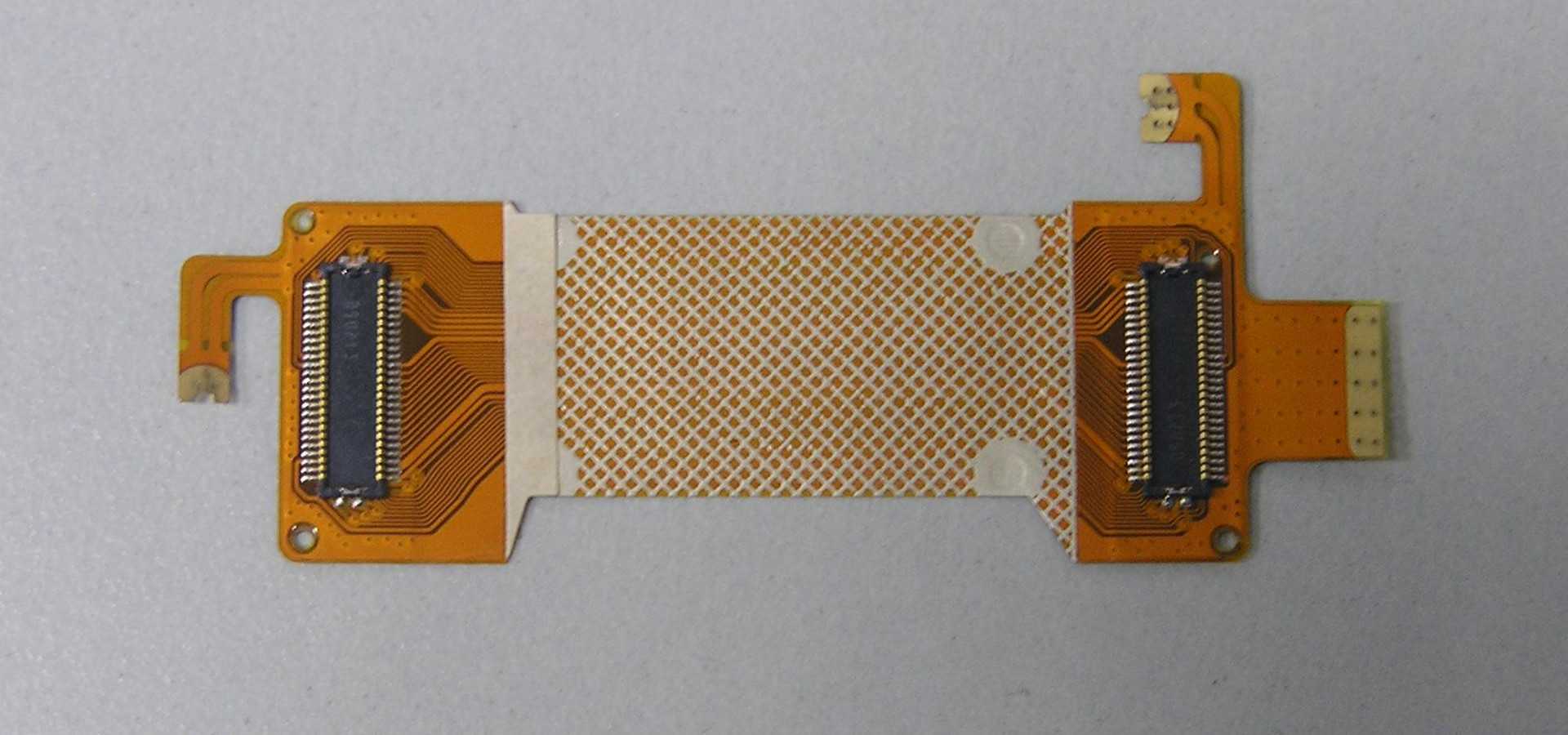
Kapton Flex Circuit Construction
Kapton flex circuits have three basic component layers:
Polyimide Substrate
This Kapton film forms the flexible foundation to support the conductive traces. The thickness ranges from 1 to 15 mils (25 to 380 microns) depending on the application. Thinner material allows for tighter bend radii while thicker provides better dimensional stability.
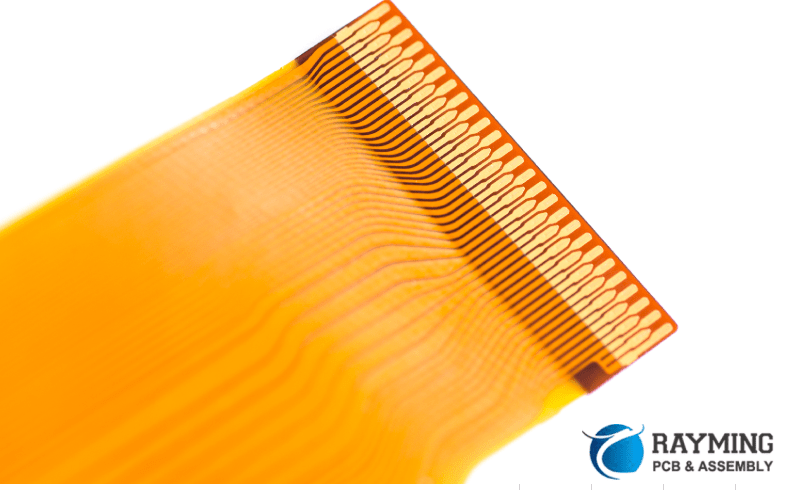
Conductive Traces
Usually made from rolled annealed copper foil around 1 oz (35 microns) thickness laminated onto the Kapton layer. The copper is etched using photolithographic processes to produce the circuit traces and patterns. Other conductor materials like aluminum or nickel alloys may also be used.
Coverlayer
An additional layer of Kapton film that bonds to the substrate around the edges of the circuit traces. This protects the traces from damage and prevents shorts. The coverlayer typically ranges from 0.5 to 3 mils (12 to 76 microns) thick. Openings in the coverlayer provide connections points between traces and components.
Other secondary layers such as stiffeners, shields, or adhesive layers can be added to tailor the flex circuit for specific mechanical, electrical, or assembly requirements.
Cross Section of a Typical Kapton Flex Circuit
The functional layers are built up through an additive photographic process using vacuum deposition and etching techniques to produce fine line trace geometries. Rolled annealed copper provides the ductility for Kapton flex circuits to flex without damage.
Kapton Flex Circuit Applications
Some common applications that benefit from Kapton polyimide-based flex circuit technology include:
Wearable Electronics
- Flexible circuits for smart watches, health monitors, augmented reality glasses
- Lightweight, comfortable fit on the body
- Withstands bending and repeated flexing
Medical Devices
- Miniature flexible circuits used in hearing aids, cochlear implants
- Catheter-based electronic assemblies for imaging, ablation, sensing
- Implantable circuits interface with body tissues
Automotive Electronics
- Flex circuits for under-hood temperature, pressure sensing
- Circuits in seats for position, temperature, weight sensing
- Flexible interconnections for mirrors, lights, sensors
Consumer Electronics
- Flexible circuits inside smartphones, laptops, game controllers
- Allows more efficient space utilization
- Dynamic flexing in headphones, robotic toys
Aerospace and Defense
- Used in guidance systems, radars, engine controls, satellites
- Withstands vibration, shock, temperature extremes
- Replaces bulky wire harnesses for weight savings
Kapton’s robustness supports mission-critical performance across a wide range of commercial, industrial, aerospace and defense applications.
Design Considerations for Kapton Flex Circuits
Here are some of the important design factors when working with Kapton flex circuits:
Flexibility
The minimum bend radius determines how tight a flex circuit can be folded without damaging the traces. This is a function of the substrate thickness, copper thickness, and flex circuit layer count. Dynamic flex applications require higher flexibility than static bends.
Routing Density
Thinner dielectric films allow higher trace densities and more complex routing in multi-layer flex stacks. Common substrates are 1 to 5 mil thick for standard trace/space widths from 0.5mm (20 mil) and below.
Rigid Sections
Discrete components often mount to rigid islands on the flex circuit. Stiffeners help minimize distortions during assembly. Thermal expansions between flex and rigid sections require analysis.
Connections
Smaller pad sizes and pitches, microvias, and staggered connections support high I/O density. Soldering, bonding, connectors, or elastomeric interconnections attach flex circuits.
Safety Margins
It’s important to de-rate Kapton material properties when designing. Allow safety margins on bend radii, current capacities, voltages, temperatures, and other parameters.
Reliability Testing
Simulate extreme environment exposures during design verification. Accelerated flex testing helps reveal failure modes before production. IPC standards provide test method guidelines.
Thorough electrical, mechanical, thermal, and assembly analysis ensures Kapton flex circuits perform reliably in their operating environments.
Kapton Flex Circuit Design Process
The design process for Kapton flex circuits involves:
- Defining circuit performance requirements
- Evaluating substrate materials and constructions
- Developing initial layout and routing
- Optimizing trace widths and clearances for current and voltages
- Determining minimum bend radii for flex and dynamic regions
- Adding stiffeners and strain reliefs as needed
- Analyzing thermal loads and expansion effects
- Modeling mechanical stresses from motion, vibration, shock
- Designing appropriate interconnections and pads
- Developing test methods to verify reliability
CAD tools and analysis software help optimize flex circuit designs. Prototyping and testing refine the design prior to full production.
Kapton Flex Circuit Manufacturing
Fabricating Kapton flex circuits involves the following sequence of processes:
Step 1 – Etching
A layer of copper foil is laminated to the Kapton substrate. Photoresist is applied and imaged to produce the circuit trace pattern. Etching removes unwanted copper exposing the circuit layout.
Step 2 – Bonding
Additional Kapton layers are added using adhesive or thermocompression processes. Multilayer circuits are constructed by adding repeated conductor-dielectric layers.
Step 3 – Hole Drilling
Mechanical, laser, or photolithographic drilling techniques create holes for vias or component connections. Plated through holes provide vertical interconnects between layers.
Step 4 – Plating
Electroless copper deposition coats the drilled holes creating a conductive surface for traces and vias between layers. Other platings like nickel/gold can be added.
Step 5 – Solder Mask
A polymer solder mask layer is laminated and imaged to produce solderable bonding sites. Bare copper is protected from oxidation and shorting.
Step 6 – Finishing
Various finishing steps like legend printing, electrical testing, coverlay addition, singulation into individual circuits and other optional processes complete the fabrication.
High volume roll-to-roll processing reduces costs for long flex circuits produced in reels. Discrete flex circuits use panel-based sheet fabrication techniques.
Key Advantages of Kapton Flex Circuits
To summarize, here are some of the major benefits provided by Kapton-based flex circuit technology:
- Extremely thin, lightweight, and flexible
- Tight and customizable configurations
- High reliability with dynamic flexing
- Efficient manufacturing and assembly
- Rugged performance across wide environments
- Enables miniaturization and portability
- Replaces bulky connectors and harnesses
- Allows innovative packaging designs
- Supported by extensive experience and standards
With its unique properties and advantages, Kapton has become the material of choice for reliable, high-performance flex circuits across a diverse range of markets and applications. Continued technology improvements will enable flex circuits to provide solutions for the challenges of next-generation electronic systems.
Frequently Asked Questions About Kapton Flex Circuits
What are some typical applications for Kapton flex circuits?
Some of the most common applications are in consumer electronics, wearable devices, automotive, aerospace, medical, robotics, and industrial products. Kapton flex circuits provide miniaturization, reliability, and improved design freedom needed in these markets.
How are components assembled onto Kapton flex circuits?
Soldering is the most common attachment method, allowing both leaded and surface mount components. Other assembly techniques include conductive adhesives, press-fit pins, crimping, welding/bonding, or mechanical fasteners.
What are some key design considerations for Kapton flex?
Important design factors include minimum bend radius, routing densities, managing thermal expansion differences between rigid and flex areas, electrical current capacities, mechanical stress analysis, and planning for manufacturability.
How can Kapton flex circuits improve reliability compared to rigid PCBs?
The flexible material absorbs vibrations, shocks, and stresses instead of transmitting them directly to solder joints like a rigid board. Kapton’s robust temperature range and chemical resistance also improves reliability across environments.
What CAD tools are typically used for Kapton flex circuit design?
Many PCB design packages now support flex and rigid-flex design features such as layer stacks, flex modeling, bend radius rules, and automatic folding/routing. These tools help optimize designs for manufacturability and reliability.


Leave a Reply