Introduction to PCB Etching
PCB etching is a crucial process in the manufacturing of printed circuit boards (PCBs). It involves selectively removing unwanted copper from a copper-clad substrate to create the desired conductive patterns that form the electrical connections on the PCB. This process is essential for the proper functioning of electronic devices, as it ensures that signals are routed correctly and efficiently between components.
In this comprehensive article, we will delve into the details of PCB etching, exploring its various methods, the chemistry behind it, and the steps involved in the process. We will also discuss the advantages and disadvantages of different etching techniques and provide insights into the future of PCB etching technology.
Understanding the Basics of PCB Etching
What is a PCB?
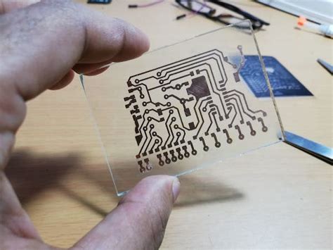
A printed circuit board (PCB) is a thin board made of insulating material, such as fiberglass or composite epoxy, with conductive copper traces printed on its surface. These traces form the electrical connections between various components, such as resistors, capacitors, and integrated circuits (ICs), which are soldered onto the board. PCBs are used in virtually all electronic devices, from smartphones and computers to industrial equipment and aerospace systems.
The Role of Copper in PCBs
Copper is the most commonly used conductive material in PCBs due to its excellent electrical conductivity, thermal conductivity, and resistance to corrosion. A typical PCB starts as a copper-clad laminate, which consists of a thin layer of copper foil bonded to one or both sides of an insulating substrate. The thickness of the copper layer can vary depending on the specific application and the desired electrical properties of the PCB.
The Need for PCB Etching
To create the desired conductive patterns on a PCB, unwanted copper must be removed from the copper-clad laminate. This is where PCB etching comes into play. By selectively removing copper, PCB etching creates the necessary electrical connections between components while ensuring that there are no short circuits or unintended connections. The accuracy and precision of the etching process directly impact the performance and reliability of the final PCB.

Methods of PCB Etching
There are several methods used for PCB etching, each with its own advantages and disadvantages. The choice of etching method depends on factors such as the desired feature size, production volume, and available resources. Let’s explore the most common PCB etching methods.
Chemical Etching
Chemical etching is the most widely used method for PCB etching. It involves using a chemical solution, called an etchant, to dissolve the unwanted copper from the substrate. The most common etchants used in chemical etching are:
-
Ferric Chloride (FeCl₃): Ferric chloride is an acidic salt that reacts with copper to form copper chloride (CuCl₂) and iron(II) chloride (FeCl₂). It is relatively safe to use and produces consistent results.
-
Cupric Chloride (CuCl₂): Cupric chloride is an alternative to ferric chloride and is known for its faster etching rates. However, it requires the addition of hydrochloric acid (HCl) to maintain its effectiveness.
-
Ammonium Persulfate ((NH₄)₂S₂O₈): Ammonium persulfate is a strong oxidizing agent that dissolves copper by converting it into copper sulfate (CuSO₄). It is less commonly used than ferric chloride and cupric chloride.
The chemical etching process typically involves the following steps:
- Cleaning the copper-clad laminate to remove any contaminants or oxidation.
- Applying a photoresist layer to the copper surface and exposing it to UV light through a photomask that contains the desired circuit pattern.
- Developing the photoresist to remove the unexposed areas, leaving the desired circuit pattern protected.
- Immersing the laminate in the etchant solution, which dissolves the unprotected copper.
- Removing the remaining photoresist layer, leaving only the desired copper traces on the substrate.
Advantages of chemical etching:
– Widely used and well-established process
– Relatively low cost
– Suitable for both prototyping and mass production
– Can achieve feature sizes down to 0.1 mm
Disadvantages of chemical etching:
– Requires handling and disposal of hazardous chemicals
– Can be time-consuming, especially for high-volume production
– Limited control over the etching process, which can lead to over-etching or under-etching
Plasma Etching
Plasma etching, also known as dry etching, is a more advanced method of PCB etching that uses a plasma (ionized gas) to remove the unwanted copper. The process takes place in a vacuum chamber and involves the following steps:
- Placing the copper-clad laminate with a patterned photoresist layer in the vacuum chamber.
- Introducing a reactive gas, such as chlorine (Cl₂) or sulfur hexafluoride (SF₆), into the chamber.
- Applying a high-frequency electric field to ionize the gas, creating a plasma.
- The reactive ions in the plasma attack and remove the exposed copper, leaving the desired circuit pattern intact.
Advantages of plasma etching:
– Achieves finer feature sizes (down to 0.05 mm) compared to chemical etching
– Offers better control over the etching process, resulting in more precise and uniform etching
– Produces less waste and is more environmentally friendly than chemical etching
Disadvantages of plasma etching:
– Higher equipment and operating costs compared to chemical etching
– Requires specialized knowledge and training to operate the equipment
– May not be cost-effective for low-volume production or prototyping
Laser Etching
Laser etching is a relatively new method of PCB etching that uses a high-power laser to remove the unwanted copper from the substrate. The process involves the following steps:
- Placing the copper-clad laminate in the laser etching machine.
- Programming the machine with the desired circuit pattern.
- The laser beam selectively vaporizes the copper, leaving the desired circuit pattern on the substrate.
Advantages of laser etching:
– Achieves very fine feature sizes (down to 0.01 mm)
– Offers high precision and repeatability
– Requires no photoresist or chemical etchants, making it a more environmentally friendly option
– Suitable for rapid prototyping and small-batch production
Disadvantages of laser etching:
– High equipment costs
– Slower than chemical etching for high-volume production
– May require post-processing to remove any debris or oxidation caused by the laser

The Chemistry of PCB Etching
To better understand the PCB etching process, it is essential to explore the underlying chemistry involved. In this section, we will focus on the most common etchant used in chemical etching: ferric chloride.
The Reaction between Ferric Chloride and Copper
Ferric chloride (FeCl₃) is an acidic salt that dissolves copper through a redox reaction. The overall reaction can be represented as:
2 FeCl₃ + Cu → 2 FeCl₂ + CuCl₂
In this reaction, the ferric ion (Fe³⁺) is reduced to the ferrous ion (Fe²⁺), while the copper (Cu) is oxidized to copper(II) ion (Cu²⁺). The resulting copper chloride (CuCl₂) is soluble in the etchant solution and is easily removed from the substrate.
Factors Affecting the Etching Rate
Several factors can influence the etching rate and the quality of the etched PCB. These include:
-
Temperature: Higher temperatures generally increase the etching rate, as they accelerate the chemical reaction between the etchant and the copper. However, excessively high temperatures can lead to over-etching and loss of feature resolution.
-
Concentration: The concentration of the etchant solution directly affects the etching rate. Higher concentrations of ferric chloride result in faster etching, but can also increase the risk of over-etching.
-
Agitation: Agitating the etchant solution helps to remove the dissolved copper and replenish the etchant at the copper surface, leading to faster and more uniform etching.
-
Etchant Regeneration: As the etching process progresses, the etchant solution becomes saturated with copper ions, which can slow down the etching rate. To maintain the effectiveness of the etchant, it may be necessary to regenerate it by oxidizing the ferrous ions back to ferric ions using methods such as aeration or the addition of oxidizing agents like hydrogen peroxide (H₂O₂).

The PCB Etching Process: Step by Step
Now that we have covered the basics of PCB etching and the chemistry involved, let’s walk through the step-by-step process of chemically etching a PCB using the photoresist method.
-
Design the PCB: Create the desired circuit pattern using PCB design software, such as Eagle, KiCad, or Altium Designer.
-
Print the photomask: Print the circuit pattern onto a transparent film using a high-resolution printer. This film will serve as the photomask during the exposure process.
-
Clean the copper-clad laminate: Thoroughly clean the copper surface of the laminate using a mild abrasive cleanser and a soft brush to remove any contaminants or oxidation. Rinse the laminate with water and dry it completely.
-
Apply the photoresist: Apply a thin, uniform layer of positive photoresist to the copper surface using a spin coater or a foam brush. Ensure that the entire surface is covered and that there are no bubbles or irregularities in the photoresist layer.
-
Soft bake: Place the laminate in an oven or on a hotplate to soft bake the photoresist. This step helps to evaporate any remaining solvents and improves the adhesion of the photoresist to the copper surface. The baking temperature and duration depend on the specific photoresist used.
-
Expose the photoresist: Place the photomask on top of the photoresist-coated laminate and expose it to UV light for the recommended exposure time. The UV light will cause the exposed areas of the photoresist to become soluble in the developer solution.
-
Develop the photoresist: Immerse the exposed laminate in a developer solution, which will dissolve the exposed areas of the photoresist, revealing the underlying copper. Gently agitate the solution to ensure even development. Rinse the laminate with water to stop the development process.
-
Hard bake: Place the developed laminate in an oven or on a hotplate to hard bake the remaining photoresist. This step improves the resistance of the photoresist to the etchant solution and helps to maintain the integrity of the circuit pattern during etching.
-
Etch the PCB: Immerse the laminate in the prepared etchant solution, such as ferric chloride, and agitate gently. Monitor the etching progress closely to avoid over-etching. Once the unwanted copper has been completely removed, remove the laminate from the etchant and rinse it thoroughly with water.
-
Remove the photoresist: Use a photoresist stripper or a solvent, such as acetone, to remove the remaining photoresist from the etched PCB. Rinse the PCB with water and dry it completely.
-
Inspect and test: Carefully inspect the etched PCB for any defects, such as over-etching, under-etching, or short circuits. Use a multimeter or a continuity tester to verify the electrical connections.
-
Drill holes and finish the PCB: Drill any necessary holes for through-hole components using a PCB drill or a CNC machine. Apply a solder mask and silkscreen if desired, and then cut the PCB to its final size.
Advantages and Disadvantages of PCB Etching
PCB etching is a crucial process in the manufacturing of electronic devices, but it has its own set of advantages and disadvantages. Let’s explore these in more detail.
Advantages of PCB Etching:
1. Cost-effective: PCB etching is a relatively low-cost process, especially for small to medium-scale production. It requires minimal equipment and materials compared to other PCB manufacturing methods.
-
Versatility: PCB etching can be used to create a wide range of circuit patterns, from simple single-layer boards to complex multi-layer designs. It is suitable for both prototyping and mass production.
-
Accessibility: The materials and equipment needed for PCB etching are readily available, making it possible for hobbyists and small businesses to create their own PCBs.
Disadvantages of PCB Etching:
1. Environmental concerns: Chemical etching involves the use and disposal of hazardous chemicals, such as ferric chloride, which can pose environmental and health risks if not handled properly.
-
Limited resolution: Compared to other PCB manufacturing methods, such as photolithography or laser etching, the resolution of chemically etched PCBs is limited by factors such as the etchant concentration, temperature, and agitation.
-
Time-consuming: Chemical etching can be a time-consuming process, especially for high-volume production or complex designs. The etching time depends on various factors, such as the copper thickness, etchant concentration, and temperature.
Future of PCB Etching Technology
As the demand for smaller, faster, and more complex electronic devices continues to grow, PCB etching technology must evolve to keep pace. Here are some emerging trends and developments in PCB etching:
-
Dry etching: Dry etching methods, such as plasma etching and laser etching, are gaining popularity due to their ability to achieve finer feature sizes and better control over the etching process. These methods also produce less waste and are more environmentally friendly than chemical etching.
-
Inkjet printing: Inkjet printing is a promising technology for PCB etching that uses a modified inkjet printer to directly print the etchant onto the copper surface. This method allows for more precise and localized etching, reducing the amount of etchant needed and minimizing waste.
-
Nanomaterials: The use of nanomaterials, such as graphene and carbon nanotubes, in PCB manufacturing is an area of active research. These materials have the potential to enable the fabrication of ultra-thin, flexible, and high-performance PCBs.
-
Environmentally friendly etchants: Researchers are exploring alternative, less toxic etchants to replace traditional chemicals like ferric chloride. These include organic acids, such as citric acid and acetic acid, and enzymatic etchants derived from microorganisms.
As these technologies mature, they are likely to revolutionize the PCB etching process, enabling the production of more advanced and sustainable electronic devices.
Frequently Asked Questions (FAQ)
-
What is the most common etchant used in PCB etching?
The most common etchant used in PCB etching is ferric chloride (FeCl₃). It is an acidic salt that reacts with copper to form copper chloride (CuCl₂) and iron(II) chloride (FeCl₂), effectively dissolving the unwanted copper from the substrate. -
Can I etch a PCB at home?
Yes, it is possible to etch a PCB at home using a simple chemical etching process. You will need a copper-clad laminate, a printed circuit pattern, etchant solution (such as ferric chloride), and basic safety equipment. However, it is crucial to follow proper safety guidelines and dispose of the used etchant responsibly. -
What is the difference between positive and negative photoresist?
Positive photoresist becomes soluble in the developer solution when exposed to UV light, while unexposed areas remain insoluble. This allows the exposed areas to be removed during development, revealing the underlying copper for etching. Negative photoresist, on the other hand, becomes insoluble when exposed to UV light, while unexposed areas remain soluble and are removed during development. -
How can I dispose of used etchant safely?
Used etchant, such as ferric chloride, is considered hazardous waste and should not be poured down the drain or disposed of in regular trash. Contact your local waste management authority for guidance on proper disposal methods. In some cases, the used etchant can be neutralized and precipitated, with the resulting solid waste being disposed of according to local regulations. -
What are the advantages of dry etching methods compared to chemical etching?
Dry etching methods, such as plasma etching and laser etching, offer several advantages over traditional chemical etching. These include finer feature sizes, better control over the etching process, and reduced environmental impact. However, dry etching methods typically require more advanced and expensive equipment, making them more suitable for high-volume production and specialized applications.
Conclusion
PCB etching is a fundamental process in the manufacturing of electronic devices, enabling the creation of conductive patterns that form the backbone of modern technology. By selectively removing unwanted copper from a substrate, PCB etching allows for the precise and efficient routing of electrical signals between components.
This article has provided a comprehensive overview of PCB etching, covering its basics, methods, chemistry, and step-by-step process. We have also discussed the advantages and disadvantages of PCB etching and explored the future of this technology, including emerging trends such as dry etching, inkjet printing, and the use of nanomater


Leave a Reply