Introduction to Multilayer PCB Boards
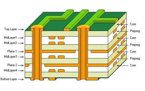
Multilayer PCB boards have become increasingly popular in the electronics industry due to their ability to accommodate complex circuitry in a compact form factor. These boards consist of multiple layers of conductive copper foil separated by insulating dielectric material. By utilizing multiple layers, designers can create more intricate designs with higher component density and improved signal integrity compared to single or double-layer boards.
However, despite their numerous advantages, multilayer PCB boards do come with certain limitations that can pose challenges for designers and manufacturers alike. In this article, we will explore these limitations in detail and discuss potential solutions to overcome them.
Multilayer PCB Limitations
Increased Manufacturing Complexity
One of the primary limitations of multilayer PCB boards is the increased manufacturing complexity compared to simpler board designs. As the number of layers increases, so does the difficulty in ensuring proper alignment, registration, and bonding between layers. This complexity can lead to higher production costs and longer lead times.
To mitigate this limitation, manufacturers employ advanced production techniques such as precise layer alignment systems, automated optical inspection (AOI), and strict quality control measures. These methods help ensure the accuracy and reliability of multilayer boards during the manufacturing process.
Signal Integrity Challenges
Another significant limitation of multilayer PCB boards is the potential for signal integrity issues. As the number of layers increases, so does the risk of crosstalk, electromagnetic interference (EMI), and signal reflections. These issues can lead to degraded performance, reduced reliability, and even complete system failure in extreme cases.
To address signal integrity challenges, designers must carefully consider factors such as layer stack-up, material selection, and routing strategies. Proper grounding and shielding techniques, along with the use of controlled impedance traces and differential signaling, can help minimize the impact of these issues.
Thermal Management Concerns
Multilayer PCB boards also face limitations related to thermal management. As the component density and power consumption of electronic devices continue to rise, the ability to effectively dissipate heat becomes increasingly critical. Inadequate thermal management can lead to component failure, reduced lifespan, and decreased overall system reliability.
To overcome thermal management limitations, designers can employ various strategies such as the use of thermal vias, heat sinks, and specialized materials with high thermal conductivity. Proper placement of heat-generating components and the incorporation of cooling solutions like fans or liquid cooling systems can also help mitigate thermal issues.
Cost Considerations
The increased complexity and material requirements of multilayer PCB boards often result in higher production costs compared to simpler board designs. This can be a significant limitation for cost-sensitive applications or high-volume production runs.
To address cost concerns, designers can explore alternative materials, optimize layer stack-ups, and employ design for manufacturability (DFM) principles to streamline production processes. Collaborating closely with manufacturers and leveraging their expertise can also help identify cost-saving opportunities without compromising board performance or reliability.
Limited Flexibility and Repairability
Multilayer PCB boards also face limitations in terms of flexibility and repairability. Once the layers are bonded together, making modifications or repairs to internal layers becomes extremely difficult, if not impossible. This lack of flexibility can be a significant drawback for applications that require frequent updates or modifications.
To mitigate this limitation, designers can incorporate modular design approaches, allowing for the replacement of specific sections or components without affecting the entire board. The use of advanced rework techniques and specialized tools can also help in certain repair scenarios, although the success of such efforts is not always guaranteed.

Overcoming Multilayer PCB Limitations
Despite the various limitations associated with multilayer PCB boards, there are several strategies and approaches that designers and manufacturers can employ to overcome these challenges. Some of these solutions include:
-
Advanced Design Tools and Simulation: Utilizing advanced PCB design software with built-in simulation capabilities can help designers identify and address potential issues early in the design process. These tools can analyze signal integrity, thermal performance, and manufacturability, allowing for design optimizations before production begins.
-
Material Innovations: The development of new materials with improved electrical, thermal, and mechanical properties can help mitigate some of the limitations of multilayer PCB boards. For example, the use of low-loss dielectrics can reduce signal attenuation and improve high-frequency performance, while thermally conductive materials can enhance heat dissipation.
-
Manufacturing Process Improvements: Continuous advancements in manufacturing technologies and processes can help overcome the complexity and cost limitations of multilayer PCB boards. Automated assembly lines, high-precision alignment systems, and advanced quality control measures can streamline production and improve overall board reliability.
-
Collaborative Design Approaches: Fostering close collaboration between designers, manufacturers, and other stakeholders can help identify and address potential limitations early in the development process. By leveraging the collective expertise and experience of the team, solutions can be developed that balance performance, cost, and manufacturability.
-
Modular Design and Repairability: Incorporating modular design principles and considering repairability during the design phase can help mitigate the limitations associated with limited flexibility and repairability. By designing boards with replaceable components or sections, repairs and updates become more feasible, extending the lifespan of the overall system.

Frequently Asked Questions (FAQ)
-
Q: What is the maximum number of layers that can be used in a multilayer PCB board?
A: The maximum number of layers in a multilayer PCB board can vary depending on the manufacturing capabilities and design requirements. Most commercial PCB manufacturers can produce boards with up to 30 layers or more. However, as the number of layers increases, so does the complexity and cost of manufacturing. -
Q: Can multilayer PCB boards be used for high-frequency applications?
A: Yes, multilayer PCB boards can be used for high-frequency applications, but careful design considerations must be made to ensure signal integrity. The use of low-loss dielectrics, controlled impedance traces, and proper grounding and shielding techniques can help mitigate high-frequency signal issues. -
Q: Are there any specific design guidelines for multilayer PCB boards?
A: Yes, there are several design guidelines that should be followed when creating multilayer PCB boards. These include proper layer stack-up, signal routing strategies, power and ground plane design, via placement, and thermal management considerations. Adhering to these guidelines can help ensure optimal performance and manufacturability. -
Q: How can I minimize the cost of multilayer PCB boards?
A: There are several ways to minimize the cost of multilayer PCB boards, such as optimizing layer stack-ups, using standard materials and sizes, employing design for manufacturability (DFM) principles, and collaborating closely with manufacturers to identify cost-saving opportunities. Additionally, considering the total cost of ownership (TCO) rather than just the initial production cost can help make informed decisions. -
Q: Are there any alternatives to multilayer PCB boards for complex designs?
A: In some cases, alternative technologies such as high-density interconnect (HDI) PCBs, flexible circuits, or 3D printing can be used to address the limitations of traditional multilayer PCB boards. These technologies offer unique advantages in terms of miniaturization, flexibility, and customization, but they also come with their own set of design considerations and cost implications.

Conclusion
Multilayer PCB boards have revolutionized the electronics industry by enabling the creation of complex, high-density circuitry in compact form factors. However, these boards also come with certain limitations that designers and manufacturers must navigate to ensure optimal performance, reliability, and cost-effectiveness.
By understanding the limitations associated with increased manufacturing complexity, signal integrity challenges, thermal management concerns, cost considerations, and limited flexibility and repairability, designers can make informed decisions and employ appropriate strategies to overcome these challenges.
Through the use of advanced design tools, material innovations, manufacturing process improvements, collaborative design approaches, and modular design principles, the limitations of multilayer PCB boards can be effectively mitigated. As technology continues to advance, it is likely that new solutions and approaches will emerge to further push the boundaries of what is possible with multilayer PCB design and manufacturing.
By staying informed about the latest developments in PCB technology and working closely with experienced manufacturers, designers can leverage the full potential of multilayer PCB boards while successfully navigating their limitations. With the right strategies and solutions in place, the future of multilayer PCB design looks bright, with endless possibilities for innovation and advancement.


Leave a Reply