Introduction
Printed circuit boards (PCBs) are essential components in almost all modern electronic devices. They provide the physical foundation to mount and connect electronic components using conductive tracks etched from copper sheets laminated onto a non-conductive substrate. While the most common type of PCB uses a rigid fiberglass substrate like FR-4, flexible PCBs (flex PCBs) built on a flexible polymer substrate are growing in popularity due to their ability to bend and flex.
Transparent flex PCBs take this a step further by using fully transparent polyimide substrates and other transparent polymers as the base, allowing the assembled PCB to be practically invisible. This opens up a range of useful applications and advantages that opaque PCBs cannot provide.
What is a Transparent Flex PCB?

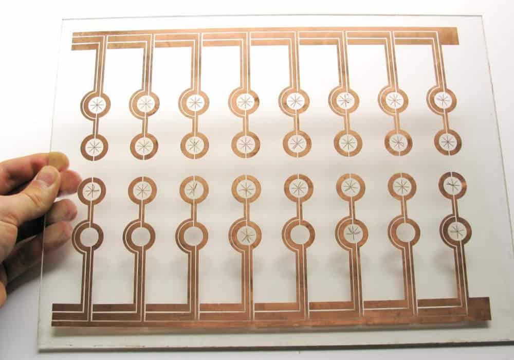
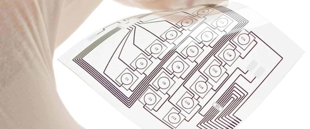
A transparent flex PCB uses a transparent polymer film like transparent polyimide as the flexible substrate. Instead of the typical copper, the conductive tracks are made from transparent conductive materials like indium tin oxide (ITO). Likewise, the solder mask layer is transparent or not applied at all. The result is a printed circuit board that is nearly invisible to the naked eye.
The main advantages of transparent flex PCBs are:
- Visually unobtrusive electronics
- Allow light to pass through the PCB
- Used for touch screens and displays
- Improved signal quality with ITO conductors
- Easier to inspect solder joints and connections
Some disadvantages are:
- More expensive than standard PCBs
- ITO conductors have higher resistance than copper
- Requires specialized transparent materials and fabrication
Typical Applications of Transparent Flex PCBs
Transparent flex PCBs are designed for applications where visibility and flexibility are important characteristics:
Touch Screens
Touch screens like those used on smartphones, tablets, and interactive kiosks require transparent flex PCBs underneath the outer glass touch layer. The PCB connects the touch sensors to the main device logic board. A stiff PCB would be visible obscuring the screen and unable to wrap around the edges.
Displays
Small LED or OLED displays are often built on transparent flex PCBs to allow the light to shine through unimpeded. They provide electrical connections and mounting points for the display components while remaining unseen behind the pixels.
Wearable Technology
As wearable devices like smart watches and fitness trackers become more popular, transparent flex PCBs allow them to be lighter and more comfortable to wear. The PCB can conform to the wearer’s body shape.
Medical Devices
For implants or on-skin medical devices like EKG monitors, transparent flex PCBs are ideal for bio-compatibility and visibility of the skin underneath. The flexibility also allows the PCB to move naturally with the skin.
Automotive Displays
Dashboard displays, rear view cameras, and other automotive electronics use transparent PCBs to mount components without blocking visibility. They can also handle the vibration and mechanical stress in vehicle environments.
Materials Used in Transparent Flex PCBs

To fabricate a high quality transparent flex PCB requires specialized materials designed for optical clarity, flexibility, and reliable performance. Here are some of the main materials involved:
Substrate
The flexible transparent substrate gives the PCB its mechanical properties. Common options are:
- Polyimide (PI) – This colorless polyimide film is the most popular choice. It has excellent optical clarity along with thermal and chemical resistance. It remains stable and flexible at a wide range of temperatures.
- Polyethylene terephthalate (PET) – PET polymer film is more economical than polyimide but has lower maximum working temperatures. It also absorbs more moisture.
- Polyethylene naphthalate (PEN) – With similar properties to PET film, PEN offers improved temperature resistance and stability. It has lower moisture absorption than PET.
Conductors
Replacing opaque copper tracks, transparent conductors options are:
- Indium tin oxide (ITO) – This alloy of indium oxide and tin oxide is the most common transparent conductor. It provides good conductivity and optical transparency, but has higher electrical resistance than copper.
- Graphene – Graphene, made from a layer of carbon atoms in a hexagonal lattice, is an emerging transparent conductor alternative. It has excellent conductivity, flexibility, and transparency.
- Silver nanowires – Tiny silver nanowires can be layered onto the substrate to form transparent conductors. The concentration and diameter of the nanowires determines the transparency and conductivity.
- Carbon nanotubes – Similar to silver nanowires, carbon nanotubes layered onto the substrate can create transparent electrodes. However, conductivity is generally lower than ITO or graphene.
Coverlay and Solder Mask
Instead of opaque solder mask to cover copper traces, transparent flex PCBs use:
- LCP (Liquid Crystal Polymer) – A glossy transparent polymer that can provide electrical insulation and mechanical protection while remaining see-through.
- Polyimide – The same polyimide film used as the substrate can also serve as a transparent solder mask.
- No solder mask – For simple circuits, solder mask may be omitted entirely since the ITO traces do not need protection or insulation.
Fabrication of Transparent Flex PCBs
Producing transparent flex PCBs requires specialized fabrication techniques and processes to handle the unique materials while maintaining optical clarity. Here is an overview of how they are manufactured:
1. Substrate Preparation
The transparent polymer film substrate starts with an adhesion promotion treatment to prepare the surface for subsequent layers. This often involves corona treatment or chemical processes.
2. Conductive Layer Deposition
The transparent conductive layer, typically ITO or graphene, is deposited onto the substrate through methods like sputtering or chemical vapor deposition (CVD). The thickness and deposition conditions determine the conductivity.
3. Photolithography
Using photoresist and standard lithographic processes, the conductor layer is etched to form the desired circuit pattern. Precise control prevents any etching residue from impacting transparency.
4. Dielectric Layer Addition
If required, a thin transparent dielectric layer like LCP can be added to provide electrical insulation between layers in multilayer boards. Additional conductor layers are then added and etched if needed.
5. Component Assembly
Components are soldered onto the board using transparent solder or conductive adhesives. Careful process control prevents any residue buildup or contamination.
6. Final Testing
The finished transparent flex PCBs undergo electrical testing and optical inspection to verify full functionality, reliability, and clean transparency without any defects or contaminants.
Pros and Cons of Transparent Flex PCBs
Here are some key advantages and disadvantages when considering using transparent flex PCBs:
Advantages:
- Visually unobtrusive electronics integration
- Allow embedded lighting or displays
- Flexibility and conformability unmatched by rigid PCBs
- Usable in wearable devices and medical equipment
- Enable touch screens and touch panels
- Improved RF performance with ITO traces
Disadvantages:
- More expensive to fabricate than standard PCBs
- Limited number of specialized manufacturers
- ITO has higher resistivity than copper traces
- Typically only 1-2 conductive layers are possible
- Sensitive to contamination affecting visual clarity
- Require careful handling and installation
Future Outlook on Transparent Flex PCBs
With the growing prevalence of displays, touch interfaces, wearables, and transparent electronics, the market demand for transparent flex PCBs is increasing each year. Improving fabrication techniques and new material developments will further improve the capabilities and adoption of transparent flex PCBs.
Graphene and silver nanowires are emerging to complement and possibly supersede ITO as the conductor of choice, offering higher conductivity and lower cost. Transparent dielectrics and substrates are also improving. This will enable more multilayer transparent boards and applications.
Higher volume manufacturing along with technology improvements will help make transparent flex PCBs more affordable and available. This will accelerate their use for displays, touch screens, imagers, sensors, and other see-through electronics.
Conclusion
As electronic products become more integrated into our environment and physical lives, transparent flex PCBs provide the enabling technology to make circuits and components practically disappear. This allows the creation of interfaces and electronics that seamlessly overlay and interact with our world. While still a specialty technology, transparent flex PCBs are now accessible and reliable enough for integration into consumer and industrial products.
Frequently Asked Questions
What are the main advantages of transparent flex PCBs?
The advantages of transparent flex PCBs include visual unobtrusiveness, ability to embed lighting or displays, excellent flexibility and conformability, suitability for wearable devices, and enabling technologies like touch screens and sensors.
What are some typical applications for transparent flex PCBs?
Typical applications that benefit from transparent flex PCBs include touch screens, displays, wearable electronics, medical devices, car electronics, and any area where see-through circuit boards are desired.
What special materials are used to fabricate transparent flex PCBs?
Specialized materials include transparent polymers like polyimide for the flexible substrate, transparent conductors such as ITO or graphene for the conductive layers, and transparent coatings like LCP as solder mask.
How are transparent flex PCBs fabricated?
Fabrication involves processes like sputtering for conductors, photolithography, thin dielectric layers, transparent solders, and careful handling to maintain optical cleanliness.
What are the main disadvantages or limitations of transparent flex PCBs?
Disadvantages include higher costs than standard PCBs, limited number of layers, potential contamination, and greater care needed in handling and installation. ITO’s lower conductivity than copper is also a tradeoff.
What does the future look like for transparent flex PCB technology?
The technology is improving quickly with advances in materials, fabrication, and cost reductions. This will enable wider adoption in consumer electronics and other applications as transparent flex PCB capabilities grow.


Leave a Reply