Introduction to Blind Microvias
Blind microvias are a type of interconnect technology used in high-density printed circuit boards (PCBs) to increase the integration density and minimize the size of the board. Unlike traditional through-hole vias that span the entire thickness of the PCB, blind microvias only extend from the surface to a specific inner layer, allowing for more efficient use of space and improved signal integrity.
What are Blind Microvias?
Blind microvias are small, laser-drilled holes that connect the outer layer of a PCB to one or more inner layers, without penetrating through the entire board thickness. These microvias are typically smaller than 150 microns in diameter and are filled with conductive material, such as copper, to establish electrical connections between layers.
Advantages of Blind Microvias
The use of blind microvias offers several advantages in PCB design and manufacturing:
- Increased integration density: By utilizing the inner layers of the PCB, blind microvias enable more components and interconnects to be placed on a smaller board area.
- Improved signal integrity: Shorter interconnects provided by blind microvias reduce signal attenuation and distortion, leading to better overall signal quality.
- Reduced layer count: With blind microvias, designers can often reduce the number of layers in a PCB, resulting in a thinner and more cost-effective board.
- Enhanced thermal management: Blind microvias can be used to create thermal vias, which help dissipate heat from high-power components more efficiently.
Manufacturing Process of Blind Microvias
The manufacturing process of blind microvias involves several key steps to ensure high-quality and reliable interconnects.
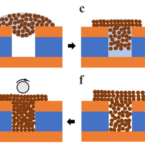
Step 1: Laser Drilling
Blind microvias are typically created using laser drilling technology. A focused laser beam is used to ablate the dielectric material and create a precise, small-diameter hole from the surface to the desired inner layer. The most common laser types used for this process are UV and CO2 lasers.
Step 2: Desmear and Cleaning
After laser drilling, the microvia holes undergo a desmear process to remove any resin or debris from the hole walls. This step is crucial to ensure proper adhesion of the conductive material during the plating process. The desmear process typically involves a combination of chemical and plasma treatments.
Step 3: Electroless Copper Deposition
Once the microvias are cleaned, an electroless copper deposition process is used to create a thin, conductive seed layer on the hole walls. This seed layer serves as a foundation for the subsequent electrolytic copper plating process.
Step 4: Electrolytic Copper Plating
The PCB is then subjected to an electrolytic copper plating process, which deposits a thicker layer of copper onto the seed layer, filling the microvia and creating a robust electrical connection between the layers.
Step 5: Planarization
After plating, the surface of the PCB may be slightly uneven due to the presence of the filled microvias. A planarization process, such as chemical-mechanical polishing (CMP), is used to level the surface and ensure a smooth, even topography for subsequent processing steps.

Design Considerations for Blind Microvias
When incorporating blind microvias into a PCB design, several key factors must be considered to ensure optimal performance and manufacturability.
Via Size and Aspect Ratio
The size and aspect ratio of the blind microvias are critical design parameters. Smaller via diameters allow for higher integration density but may pose manufacturing challenges. The aspect ratio, which is the ratio of the via depth to its diameter, should be kept within manufacturable limits to ensure reliable plating and filling of the microvias.
Via Placement and Spacing
The placement and spacing of blind microvias should be carefully considered to avoid signal integrity issues and manufacturing defects. Designers should adhere to the minimum spacing requirements between microvias and other features, such as traces and components, to prevent shorting and ensure proper insulation.
Layer Stack-up and Material Selection
The choice of layer stack-up and materials plays a significant role in the successful implementation of blind microvias. The dielectric materials should have suitable properties, such as low dielectric constant and low loss tangent, to minimize signal attenuation and distortion. The copper foil thickness and surface finish should also be selected based on the specific requirements of the application.
Signal Integrity Analysis
Signal integrity analysis is essential when designing high-speed PCBs with blind microvias. Designers should perform simulations and modeling to assess the impact of microvias on signal propagation, crosstalk, and impedance matching. This analysis helps optimize the design and ensure reliable performance across the desired frequency range.

Applications of Blind Microvias
Blind microvias find extensive use in various applications that demand high-density interconnects and miniaturization.
Consumer Electronics
The consumer electronics industry heavily relies on blind microvias to create compact, feature-rich devices such as smartphones, tablets, and wearables. These devices require high-density PCBs to accommodate the increasing number of components and functions within a limited space.
Automotive Electronics
As vehicles become more sophisticated and electrified, the use of blind microvias in automotive electronics has grown significantly. Advanced driver assistance systems (ADAS), infotainment systems, and electric vehicle power electronics all benefit from the increased integration density and improved signal integrity offered by blind microvias.
Medical Devices
Medical devices, such as implantable sensors and wearable health monitors, require highly miniaturized and reliable PCBs. Blind microvias enable the development of compact, high-performance medical electronics that can withstand the stringent requirements of the healthcare industry.
Data Centers and Networking Equipment
High-speed networking equipment and data center infrastructure rely on blind microvias to achieve the necessary signal integrity and bandwidth for high-frequency applications. Blind microvias are used in backplanes, switches, routers, and other critical components to enable faster data transmission and processing.

Future Trends in Blind Microvia Technology
As the demand for higher integration density and performance continues to grow, blind microvia technology is expected to evolve to meet these challenges.
Smaller Via Sizes
The trend towards smaller via sizes is set to continue, with the industry pushing for sub-50-micron diameter microvias. This will enable even higher interconnect densities and further miniaturization of electronic devices.
Advanced Materials
The development of advanced dielectric materials with lower dielectric constants and improved thermal properties will support the implementation of blind microvias in high-frequency and high-power applications. These materials will help minimize signal loss and ensure reliable performance in demanding environments.
3D Integration
The use of blind microvias will play a crucial role in the adoption of 3D integrated circuit (3D IC) packaging technologies, such as through-silicon vias (TSVs) and interposers. Blind microvias will enable the vertical stacking of multiple dies and components, leading to higher integration density and reduced package sizes.
Autonomous Vehicles
As autonomous vehicles become more prevalent, the demand for high-density, reliable PCBs with blind microvias will increase significantly. These vehicles will require advanced sensor systems, high-speed data processing, and robust connectivity, all of which will benefit from the use of blind microvias in their electronic subsystems.
Frequently Asked Questions (FAQ)
- What is the difference between blind and buried microvias?
-
Blind microvias extend from the surface of the PCB to a specific inner layer, while buried microvias connect two or more inner layers without reaching the surface of the board.
-
Can blind microvias be used in high-temperature applications?
-
Yes, blind microvias can be used in high-temperature applications, provided that the appropriate materials and manufacturing processes are employed. High-temperature dielectric materials and compatible plating processes ensure reliable performance in elevated temperature environments.
-
What are the challenges associated with manufacturing blind microvias?
-
Some of the challenges include maintaining precise via diameters and aspect ratios, ensuring proper plating and filling of the microvias, and achieving a smooth surface finish after the planarization process. Strict process control and advanced manufacturing techniques are necessary to overcome these challenges.
-
How do blind microvias impact the cost of PCB manufacturing?
-
The incorporation of blind microvias typically increases the cost of PCB manufacturing due to the additional processing steps and the need for specialized equipment. However, the cost impact can be offset by the benefits of higher integration density, reduced layer count, and improved performance.
-
Can blind microvias be used in flexible PCBs?
- Yes, blind microvias can be used in flexible PCBs, enabling high-density interconnects in applications that require flexibility and conformability. However, the design and manufacturing processes for flexible PCBs with blind microvias may differ from those used for rigid boards, taking into account the unique mechanical and thermal properties of flexible substrates.
Conclusion
Blind microvias have revolutionized the PCB industry by enabling higher integration density, improved signal integrity, and miniaturization of electronic devices. As technology continues to advance, the demand for blind microvias in various applications, from consumer electronics to automotive and medical devices, is expected to grow significantly.
By understanding the manufacturing process, design considerations, and future trends in blind microvia technology, engineers and manufacturers can harness the full potential of this interconnect solution to create innovative, high-performance PCBs that meet the ever-increasing demands of the electronics industry.
As the adoption of blind microvias continues to expand, it is crucial for professionals in the PCB industry to stay up-to-date with the latest advancements and best practices in design and manufacturing. This will ensure the successful implementation of blind microvias in a wide range of applications, driving the future of electronic packaging and interconnect technology.


Leave a Reply